This thread has been locked.

If you have a related question, please click the "Ask a related question" button in the top right corner. The newly created question will be automatically linked to this question.

TPS27801A output voltage glitch

Genius 3870 points
Other Parts Discussed in Thread: TPS27082L, TPS27081A, TPS22965

Hi Mr !

I met the same problem and learned  some very useful information from your simulation in this post:

e2e.ti.com/.../919286

However, I have question about this simulation result.

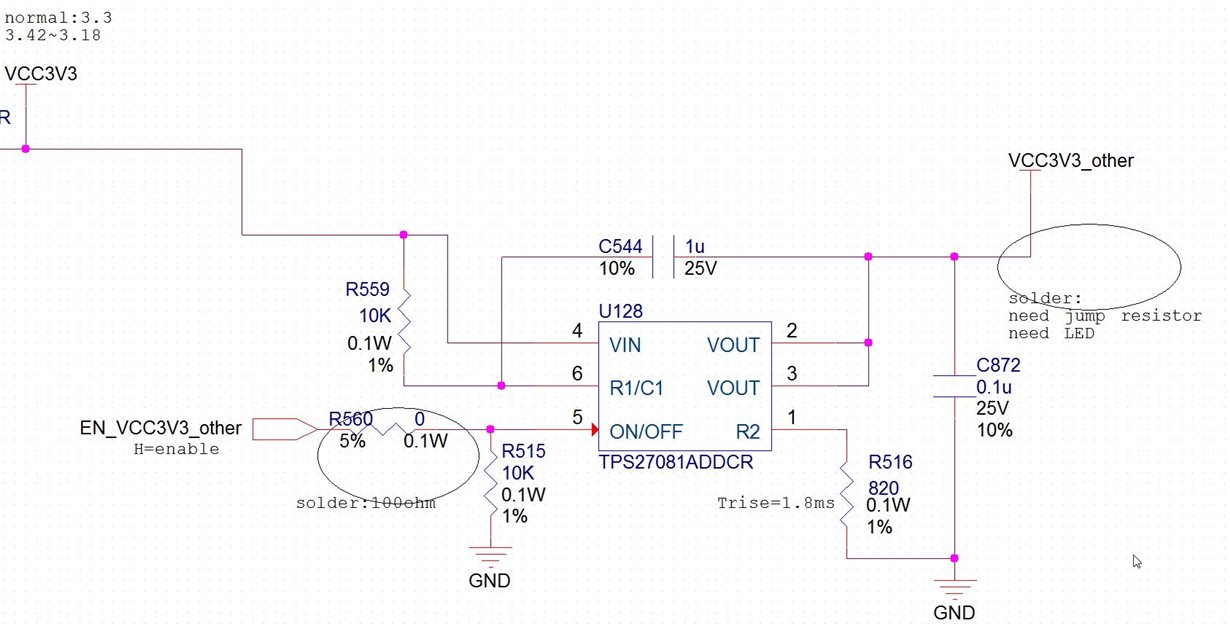
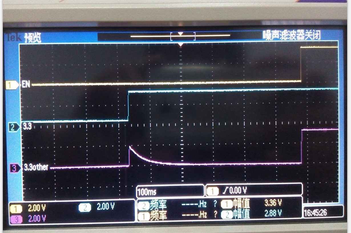
I understand there'll be a giltch when VIN is supplied to loadswitch, BUT after a while, the R1C1 pin's voltage shall be gradually charged to VIN through R1 and C1, so the PMOS with turn off. the output voltage should be 0Vrather than 0.8V. How do you see my analysis? the following is my sch and test waveform(CH1 is Enable, CH2 is VIN, CH3 is VOUT ). 

some more question, could you please help? Thanks a lot!

(1) As you suggested, the TPS27802L have better OFF performance as "The TPS27082L will short out R1 with ON/OFF pin is low."  but I did not  found this information in 082L's datasheet. The probably similar description is in section 8.2.2.4:"When a capacitor C1 is present the VIN to VOUT coupling is capacitive and is set by the C1 to CL capacitance ratio".  How should I interprate "set by ratio C1/CL"?

(2)compare the datasheet's front page of 081A and 082L, I found the schematic symbols of Q1 and Q2 are different in those two devices. It is clear that 082L uses Enhancement MOSFET while the 081A uses JFET? I am not sure about this .....

  • Hi Yi,

    This question now belongs in the "Load Switches" forum. I will move this thread accordingly.

    Thanks,
    Alex
  • Thanks, Alex.
    May I ask when will you company enter Christmas holidays ? and during this period, the forum answering from TI experts may stop?
  • Hello Yi,

    1) We don't have lab data to define this well, just that the TPS27082L will suppress the glitch from VIN to VOUT when the ON/OFF pin is OFF. A larger C1 capacitance relative to the load capacitance will couple less transient to the output.

    2) You are correct that the two devices are based on the same architecture.

    As for Christmas holiday, we have our holiday on December 24-25 as well as January 1. Typically, posts will not be answered during the holidays, but someone may be monitoring the forum.

    Best,
    Michael
  • Hi Micheal, thanks for your answer.

    (1)I am confused,  without lab data, the datasheet did claim in section 8.2.2.4 that "TPS27082L architecture helps isolate fast transients at the VIN when PFET is in the OFF state", could you please tell me why 082L is better than 081A on this feature? I mean, from the design principle prospective, how will 082L supress the transient while 081 can't ?

    on ther other hand, I have different view with yours on C1 , as section 8.2.2.4 says "When a capacitor C1 is present the VIN to VOUT coupling is capacitive and is set by the C1 to CL capacitance ratio", so I think the a smaller C1 will couple less transient to VOUT. There is actually a C1 and CL divider relationship here.

    (2)Since these two devices are using same architecture, why their schematic symbols on page one of datasheets are different?

    (3)Now we met the "glitch from VIN to VOUT when the ON/OFF pin is OFF" problem but at the same time we need soft start feature. here is a delimma in choosing C1. Does TI has any other loadswtich could satisfy our requirements: no gitch , and have soft-start control?

    Thanks again.

  • Yi,

    1) The TPS27081A is just a NMOS+PMOS switch. Nothing more, nothing less.

    The TPS27082L has more circuitry. The data sheet front page says "TPS27082L features a novel OFF isolation circuit that prevents PMOS from turning ON in applications that may have fast transients, at the VIN pin when the load switch is in the OFF-state."

    The functional block diagram doesn't show the additional circuitry.

    Yes, I stand corrected. I made a mistake before. A smaller C1 will couple less transient to VOUT.

    2 ) This is a mistake in the representation of the datasheet. These two devices are the same, except the TPS27082L has the additional circuitry mentioned. We are working to update both of these datasheets in the near future.

    3) There is another team that has additional load switches that may be able to satisfy what you need. I will reach out to them and have them answer this post with any suggestions they may have.

    Best,
    Michael
  • Hi Yi,

    TI offers several other load switches which may satisfy your conditions, all members of the TPS229xx family.  For a 3.3V rail, you may want to take a look at the TPS22915C or TPS22965.

    The TPS22915C is a simple, 0.76mm x 0.76mm device will a controlled rise time of 800us.  It can handle currents up to 2A and voltages up to 6V.

    The TPS22965 is a 2mm x 2mm device which has an adjustable rise time governed by an external capacitance.  It can handle currents up to 6A and voltages up to 6V. 

    Do either of these switches sound like they could be a solution here?

    Thanks,

    Alek Kaknevicius

  • Thanks Alek. I will see which one we could use.
  • Thanks for your patient answers, Michael.