This thread has been locked.

If you have a related question, please click the "Ask a related question" button in the top right corner. The newly created question will be automatically linked to this question.

TPS2350: Power supply redundancy requirement

Part Number: TPS2350

Hi, 

In our system there are two power supply one is AC to DC ( AC to DC -48 V)

In other Power supply Dc to DC ( DC is -48 Volt ) 

at a time only one supply is active, either supply coming from AC to DC board or from DC to DC board. We are using TPS2350 for both the supply , We are confuse input is -48V and we required output to +48 V can it be possible with this chip  or we will get output only -48V.Please suggest reference schematic for this.

Regards

Neelam 

  • Hi Neelam,

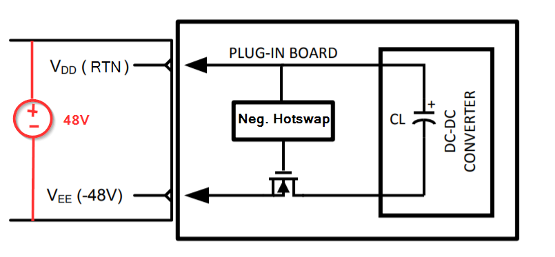
    Negative 48V means that the application uses a low-side FET for hotswap protection, and the high side is the reference node (We call it RETURN, as oppose to GND). But the voltage potential from RTN to neg 48V is still positive. The output is also a positive voltage across the output cap (look below for polarity). Below is a picture of a schematic showing a low side FET connected to a DC/DC converter. I hope this helps.

    Best Regards,

    Aramis P. Alvarez

  • Hi,

    Thanks  Aramis P. Alvarez,

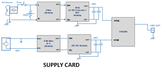
    Please find the attached block diagram of my application and suggest TPS2350 is the right choice We have two input (-48 Volts)

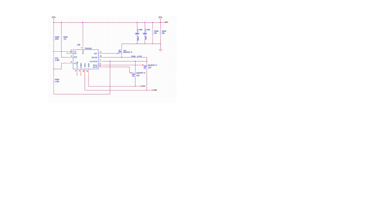
    Means input is -48 volts ( Two input -VINA and VINB- ) for negative also there is ground I am confuse about RTN with ground , -48 Volts has two terminal one is ground and other is -48 Volts i have connected ground of both the input with RTN and -48 volts Terminal with -VINa and -VINB pins , and according o you at the output at RTN pin i get +48 volts and at drain of output side MOSFET i will get ground I have attached block diagram as well as circuit of TPS2350. Please Help.

    Regards

    Neelam

  • Hi Neelam,

    I understand how this can be tricky. Neg 48V applications are meant to target telecom applications. The input supply voltage is not a negative voltage, but a positive voltage from RTN to -VIN. The reason why it's called Neg 48V is because the ground reference is on the high side (called RTN).

    With that being said, I recommend that you tie the GND of the DC/DC converters to the RTN  node. That way the device sees a positive voltage from RTN to -VIN.  I hope this helps.

    Best Regards,

    Aramis P. Alvarez

  • Hi,

    Thanks sir,

    I am attaching my schematic with this please Review it . I want 48V around@ 1 Amp Please suggest Diode at RTN for this , we are not using TP2490 with this , is it Ok. Please provide your valuable Review comments on the schematic . Please see the source pin is it Ok (Connection wise)

    Regards

    Neelam

  • Hi Neelam,

    Thank you for providing the schematic. I took a look at it and it seems that all connections look good (source connection looks correct as well). I don't believe the diode at the RTN pin is needed. Make sure that the FET's chosen have enough SOA margin for your voltage and current applications.

    For a more detailed explanation on SOA margin in hotswap controllers, please go to our app note at www.ti.com/hotswap ==> Click on “Technical Documents” ==> Click on “Robust Hot Swap”. It goes step by step to explain what the SOA/PLIM means and how it’s calculated.

    Also, you might find the EVM user's guide for the TPS2350 very helpful: http://www.ti.com/lit/ug/sluu171a/sluu171a.pdf 

  • Hi,

    Thanks Aramis P. Alvarez for your support. As input is VINA and VINB, My requirement is that if both the source are connected then it will always take from VINA and if there is any issue then it will shift to VINB.

    Is it possible with this chip? If yes please provide how it is and what changes we have to make in hardware.

    Regards

    Neelam

  • Hi Neelam,

    The supply selection n comparator selects between –VINA and –VINB based on which supply has a larger magnitude. To prevent chattering between two nearly identical supplies, the supply selection comparator has 400 mV of hysteresis. This prevents supply noise or ripple from tripping the comparator and should be adequate for most systems. Hysteresis is set to 400 mV to give the highest noise margin without allowing conduction in the body diodes of the supply selection FETs.

    The hysteresis can be increased. Please refer to page 12 of the TPS2350 datasheet for increasing the hysteresis. 

    Best Regards,

    Aramis P. Alvarez

  • Hi,

    Thanks !   400mv Deference is Ok for Our applications , Means if our VinA supply is 400mv at higher side then output is always from VINA, Is there any method in which we can sense that output current draw from which supply like from VIN A or from VINB , we want to implement a buzzer circuitry when our supply switches from A to B Please suggest 

    AS Vin A is  from AC-to DC Power supply, we set it as 1st priority

    Vin B is from DC to DC Power supply , We required buzzer when it switches from Vin A to VInB .

    Please provide reference circuitry if Possible

    Regards

    Neelam 

  • HI Neelam,

    A possible way to detect which channel is on (VINA or VINB) is to measure the voltage at each OR-ing gate (GATA and GATB). When the OR-ing channel is on it's 14V (typical) above SOURCE, and when off it's basically zero volts. Unfortunately, we do not have a reference circuit.  I hope this helps :-)

    Best Regards,

    Aramis P. Alvarez

  • Hi,

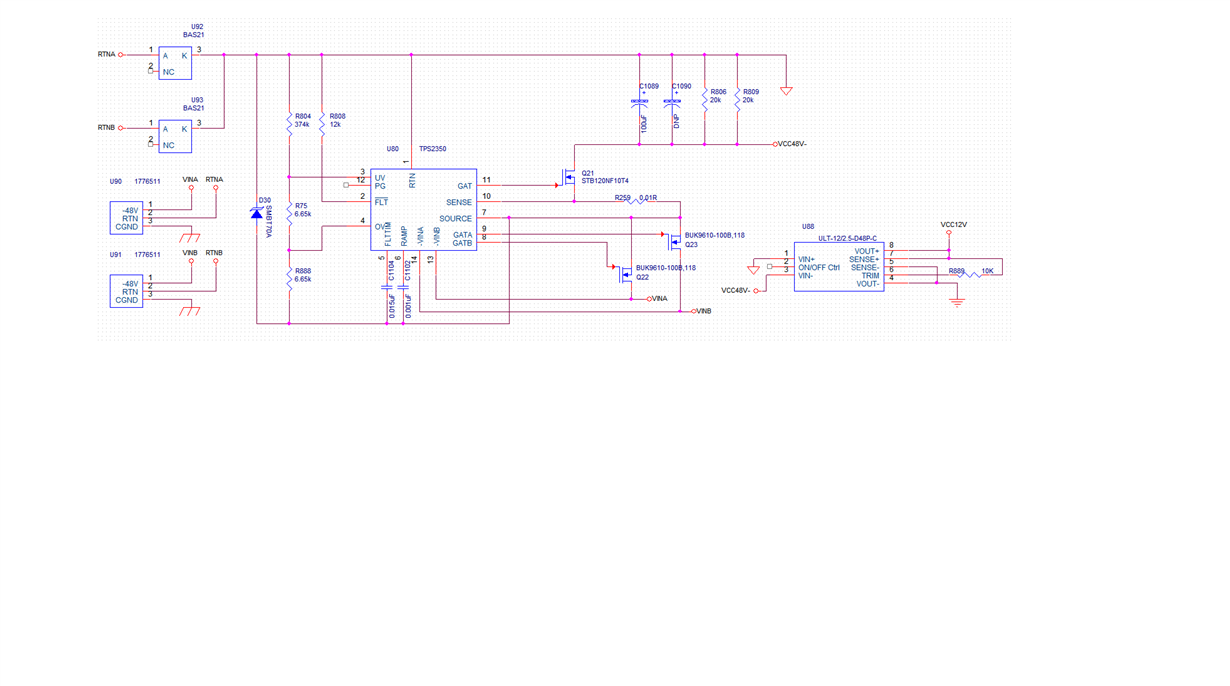
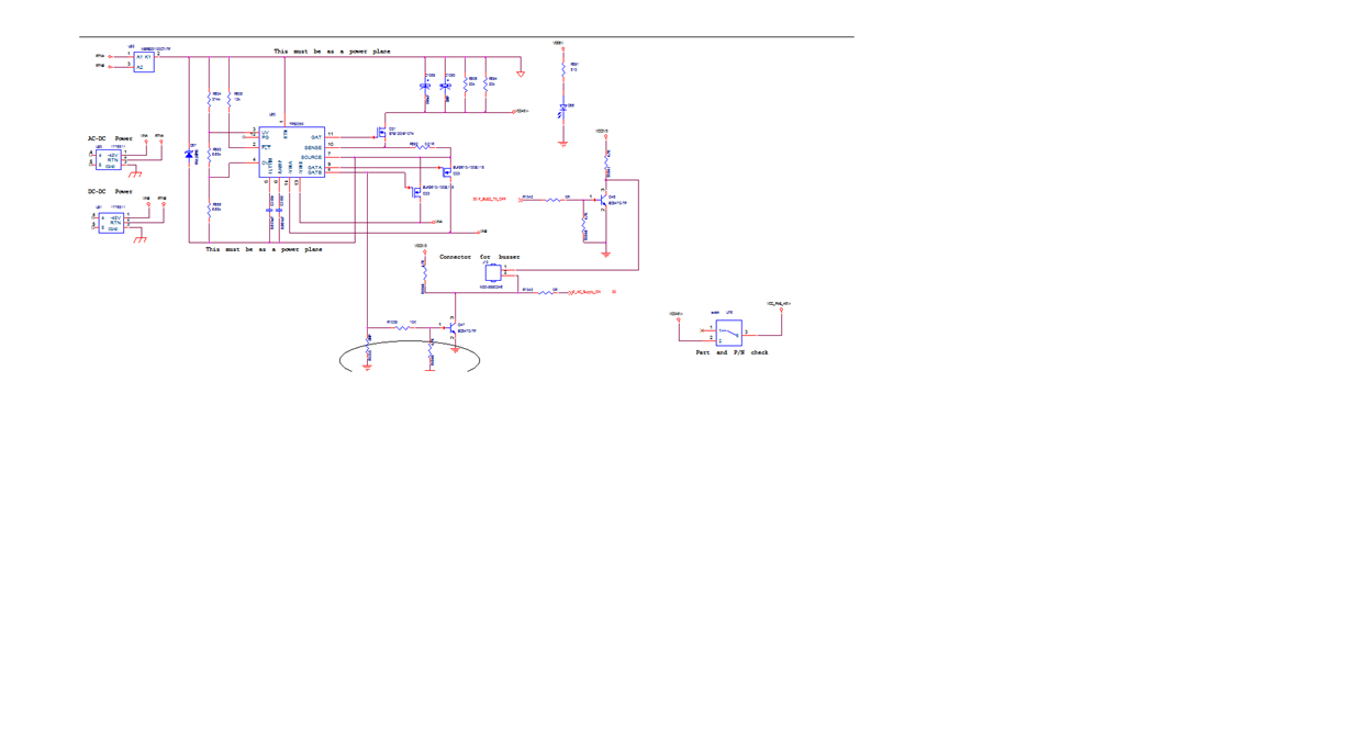
    Thanks , We have implemented some circuitry for sensing Gate voltage , Please look at the schematic is it OK

    AS per my understanding whenever Vin B is active GATE B is at 14V and It will turn on the Transistor. Please verify about ground as ground in circle are different as digital ground of the rest of the board.

    Regards

    Neelam