This thread has been locked.

If you have a related question, please click the "Ask a related question" button in the top right corner. The newly created question will be automatically linked to this question.

TIDA-00783: Gerbers layout

Part Number: TIDA-00783
Other Parts Discussed in Thread: LMZ36002, LMZ36002EVM

Hello!

I can't understand Gerbers in TIDA-00783:

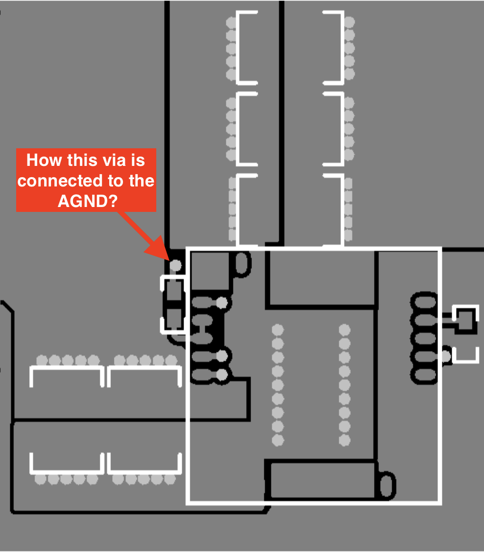
1. How R4 is connected to AGND? It's connected to via on top layer, but this via did not connected to anything on other layers.

2. In TIDA-00783: AGND and PGND are connected by via near R3. In LMZ36002 datasheet i see: "Keep AGND and PGND separate from one another. The connection is made internal to the device."

3. In pdf version of layout Mid layers are blank, but in gerbers they are not blank.

4. Can i get layout in Altium or Cadence format?

  • Hi Rustem,

    Let me take a look into this and get back to you.

    Regards,
    Jimmy
  • Hello!

    Also, plz, take a look on my implementation of TIDA-00783 layout. Is it correct (i need only 3.3V)?

    4034.Gerbers.zip

    Altium.zip

  • Hi Rustem,

    Attached is my comments regarding your layout.

    in terms of your question about the gerber file, i will get back you later.

    PCB comments.docx

    Regards,

    Yangbo

  • Hi Rustem,

    Sorry, I think the PCB file didn't include mid-layers information. We will update it as soon as possible.
    To answer your questions:
    1. R4 is connect to AGND in the mid-layer which is lost in the PCB file.
    2. In TIDA -00783, the via near R3 only connect to AGND. AGND pins are not connected together
    internal to the device and must be connected to one another externally using an analog ground
    plane on the PCB. Pins 11 and 12 are internally connected to the PGND of the device at a single
    point. The analog ground plane of the PCB should allow only analog ground currents to flow through
    these pins.
    3. The PCB file did't include the mid-layers information.
    4. Unfortunately, we can't provide the Altium files.

    Regards,
    Yangbo
  • Hello!

    Thank you for your answer!

    1. I corrected my layout, according to your comments and datasheet. Can you look again?

    7120.Altium.zip

    2. I have the same question about layout in LMZ36002 Datasheet: How R4 is connected to AGND? It's connected to via on Top layer, and this via is connected to poly on Layer 3 and Bottom Layer. But no other vias are connected to the same poly.

  • Hi, this picture is a snapshot, not complete. in the TIDA-00783 PCB file, R3 is connect to via and the via connect to AGND through a trace in the mid-layer.

  • Hi Rustem,

    The layout looks much better. In layer three, i suggest pour polygon connected to GND in the rest area. And I am guessing J11 is a test point. So where is load will connect to?

    Regards, 

    Yangbo

  • Hello!

    Here the complete module. It's have 2 options of power supply: 24 VDC or 220 VAC.

    MachineController.zip

  • Hi Rustem,

    Thanks! By the way, may i ask what is your end equipment?

    And i noticed that there are some right angle traces on the board. Is there some reasons for that? if not, i suggest do not use right angle.

    Regards!

    Yangbo

  • Hello!
    1. It's a industrial machine monitoring controller.
    2. You mean 90 degree corners? They are used only on low frequency parts of PCB.
  • Thanks Yangbo for the feedback on the LMZ36002!

    You get to play with some cool parts!

    Regarding:

    A. LMZ36002 Datasheet

    B. schematic and layout in this thread

    C. TI Reference Design TIDA-00783

    D. TI Evaluation Module LMZ36002EVM

    I am confused if the LMZ36002 already contains a high frequency bypass cap internally. TIDA-00783 adds an external 0.1uF bypass cap. LMZ36002EVM does NOT have a 0.1uF bypass cap. The datasheet does not ref to a 0.1uF either. Is the 0.1uF needed? I might be missing something and it is hard to break the habit of adding a 0.1uF before any regulator, but is it needed with the LMZ36002? or is it redundant to the internal input bypass cap?

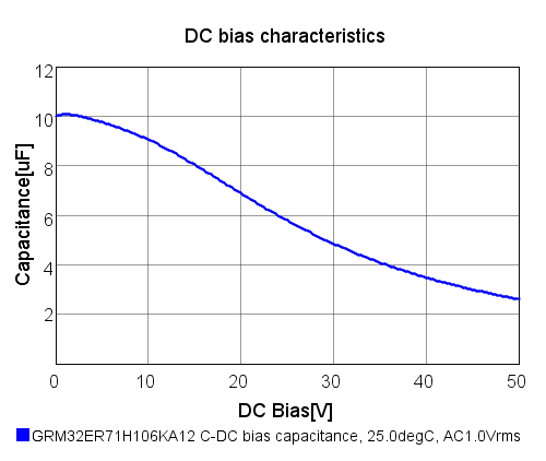
    Also, TIDA-00783 is also accompanied by test data at 40V input which is very confusing since the DC bias at 40V would reduce the effective ceramic capacitance very close to or below the minimum 4.7uF specified in the datasheet (page 7). psearch.en.murata.com/.../GRM32ER71H106KA12#.html murata link to DC Bias vs Capacitance shows <4uF@40V . How much room is there in the datasheet numbers? Is the higher ESR electrolytic capacitance able to offset the >=4.7uF requirement?

    What should I try to observe with a scope to see if I risk long term failure with capacitor aging and temperature dropping another 10% from capacitance? How can I observe not enough Vin ceramic capacitance?

    Many thanks for the feedback!

  • Hello,

    To answer your question:
    1. I would say that 0.1uF is not necessary, but you need to put the 10uF as close as possible to the module . This is not my design, so maybe I didn't see some considerations behind that.
    2. You are right, the effective value should be higher than 4.7uF to make sure the device work properly. You might don't want to use that capacitor for 40V input condition. Please follow the datasheet. Choosing a higher voltage rate or larger size capacitor will help improve the effective capacitance. The input voltage ripple will increase as the input capacitance drops. I suggest you to ask the capacitor factory for the data to meet the >=4.7uF requirement.