This thread has been locked.

If you have a related question, please click the "Ask a related question" button in the top right corner. The newly created question will be automatically linked to this question.

TPS386000: Do MR input and RESET outs have the same ESD tolerance as the analog sense ports?

Part Number: TPS386000
Other Parts Discussed in Thread: LM3880

Does the ESD rating in datasheet section 6.2 apply to all in/out pins of the device or just the sense inputs?  Is there any CMOS latchup characterization data available on the MR input and maybe the RESET outputs?

In testing some proto boards that use the TPS386000, some of the power sequence checks involve probing certain nodes of the device to verify timing.  It wasn't until about the third board that I noticed the device was not working right with respect to the MR input, and there was also a noticeable jump in idle current on subsequent power-ups following probing. 

On the very first 2 boards, after the initial probing, I measured 29-ohms and 145-ohms across the supply rail that feeds the device.  Before powering up a third board, I measured around 34K ohms across the rail.  With power ON, as I touched scope probes to MR and RESET1, I noticed the current had jumped up from around 1mA at initial power-on to around 82mA.  After a power off-on cycle, the higher current persisted, and now the rail measured around 40-ohms.  The 3.3V rail of the device is generated by a dedicated linear regulator with clean risetime and no overshoot.  The test setup is static protected (grounded benchtop stat-mat, static wriststrap, etc.) and the scope probe GND clips were clamped onto ground plane connected shells on the board. 

On the 4th board, I installed diode Vdd/Vss clamping on both pins being probed and was able to continue testing without further incident.   Subsequent unmodified boards were powered up and provisioned; those behaved normally and no extra idle current was seen since they were not probed. 

It appears the simple act of touching a high-impedance scope probe to those two nodes (not sure which one did the damage) destroyed the chip.  I've only ever seen such sensitivity on dedicated crystal osc port pins which typically do not have ESD protection.  Subsequent resistance measurements of the two nodes on board 3 showed no less impedance than the 10k pullups being used, to either rail. That suggests the damage is not directly within the input or output structures of the two pins, which could point to an induced latchup event rather than punched gate.

  • Rick,

    I believe the ESD ratings are for all in/out pins. I don't believe we have CMOS latchup characterization data for the MR input or RESET outputs but I can check with my systems and design teams. I also haven't heard of such sensitivity with the TPS386000 and I don't believe simply touching a scope probe to any of the pins will cause device damage. Could it be possible you accidentally shorted any of the pins?

    Can you describe what timing you are trying to verify and the reasoning behind the probing? I can try to figure out another way to get the information you need.

    -Michael
  • Michael

    I'm as surprised as you. There are no extraneous voltage nodes anywhere near the probe points, which were at the pullups rather than the chip pins, so accidental shorting to a voltage net with the probe tip is impossible. I could've blamed it on a finger problem if it was one card but all three were damaged identically with the same action. Then, after I added the clamp diodes, board 4 survived the same probes to the same nodes.

    The measurements are part of the first proto functional assessment and I was checking for the delay of OUTPUT1 from MR/sense1 rising. I can make those measurements at other points if need be but board 4 allowed me to get the info I needed. I was first alerted to the issue when I programmed an MCU on board 1. The device was not starting up properly and needed a manual reset to start running. I traced the problem back to the fact that the reset pin was not being held active as the MCU rail came up. The RESET1 of the 386000 is used for master reset control and should only release when MR and the SENSE1 input (which monitors the MCU rail) are high for about 4.6msec (CT1 delay time). On the damaged boards, the RESET1 output is permanently high, messing up the MCU startup but subsequent sequence steps execute with expected interstep timing so the missing first step was easy to overlook initially.

    My initial testing also started off with the main board power coming from a floating (wrt to AC hydro earth) DC supply, but the two scope probes I was using had their GND wires gripped firmly onto galvanically grounded metal shells of some nearby USB connectors, so the probe tips should not have been imparting any significant induced common-mode excursions into the probed nodes.

    I'm curious to know whether the issue is direct damage to the input or output structures of the pins being probed, or if the chip latched up somewhere deeper inside. I was expecting to see low resistance from at least one of those pins to a rail, but that's not the case.
  • Rick,

    It's tough for me to support this item because I'm still not exactly sure what you did and on what circuit configuration. I can try to replicate your testing if you can explain the setup. Your scope probes and board should be referencing the same GND though to keep all the voltages at the correct expected levels with respect to each other.

    It also sounds like you were able to protect the 4th board using external clamping diodes to get the timing info you needed. That is what we recommend when the ESD protection needs to be improved. Under normal operating conditions this should not be needed however.

    And it also sounds like there were some issues with the /RESET1 configuration and/or MCU software? Does everything work now as expected? Are there any issues that still remain?

    -Michael
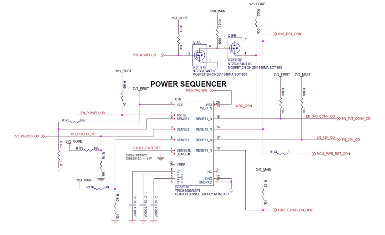
  • Here s the circuit around the monitor chip.  Briefly, the sequence starts when EN_POWER_OD is released from GND and rises high, indicating that the main bus rail is stable for the regulators to start running.  That unhooks MR, which as long as the 3V3_FIRST rail is up around 3V sensed on SENSE1, releases RESET1 after a delay time (about 4.6msec).  That action starts up the main 3V3_CORE regulator, which returns its Good status to SENSE2 (redundantly checked by the divider), releasing RESET2 after another delay.  That action allows the MCU to come up out of reset.   On the damaged chip, all RESET outputs slew up along with the rails they are pulled to, so RESET2 for instance would come up along with 3V3_CORE and the MCU would never see a valid Reset assertion during the rail slew-up.   

    Due to the arrangement of test steps, the MCU was programmed after the damaging probing had taken place and it would not run the simple first life code which was to wink an LED.  I traced the problem back to the MCU_PWR_RST_ODN signal being high well before SENSE2 was asserted.  Around the same time, I noticed the chip was drawing about 82mA and was getting physically warm to the touch.

    The scope ground gators were gripped to metal connector shells that are hard-tied to the GND plane on the board.  That is what really surprised me since I'm quite familiar with ESD control and countermeasures.  The only thing I can think of is that the probe capacitance is ringing with the GND clip wires which are about 6in long and inductive above a few 10-s of MHz.  Since this happened as I touched the circuit while live, the ringing wouldn't have to present damaging energy or be long-lived but just enough to trigger a parasitic SCR latchup.  A parasitic SCR structure can be triggered by a pulse shorter than 10nsec under the right conditions.  That could explain why the MR_N and RESET1 output measure only the pullup impedances (10K) to either rail (i.e.: don't appear to be damaged), whereas the Vcc pin is presenting 30-40 ohms to GND.   

    We have over 10 other boards in the same batch where the power sequence works as designed since the two nodes in question were not probed.  No clamping was added to any of those remaining boards and It's clear that nothing that the existing circuitry is presenting to those pins is causing the chip to fail.   

  • Rick,

    Does this mean the issue is resolved? We have also created a voltage sequencing supervisor that monitors and sequences up to 4 voltage rails using TPS386000 in addition to simple sequencer device LM3880. If you are interested in learning more about this solution or if you need any additional support or troubleshooting with your current configuration, please let me know. Thanks!

    -Michael