This thread has been locked.

If you have a related question, please click the "Ask a related question" button in the top right corner. The newly created question will be automatically linked to this question.

TPS25942A: About reverse blocking.

Part Number: TPS25942A
Other Parts Discussed in Thread: TPS25944A

Hi,
My customer has a question.

This is written in the data sheet.
[The TPS25942, TPS25944 monitor V(IN) and V(OUT) to provide true reverse blocking from output when V(IN) <(V(OUT) – 10 mV).]

But,
After checking the operation,
Following the rise in VOUT, VIN was also rising.
Is this correct behavior?

The customer is using the circuit of Figure 87.(Datasheet P44)

Best Regards,
Watanabe

  • Hi Watanabe,

    Thank you for your question and welcome to e2e. I'm going to move this thread to the appropriate forum.

    Best Regards,

    Aramis P. Alvarez

  • Hi Watanabe,

    The behavior also depends on the input capacitance of the device.
    When the device is in ON state and the input voltage is disconnected, the output hold up capacitor feeds the capacitor at the input node. This charging current from VOUT to VIN should result in more than 10mV drop across the device (i.e., VIN < VOUT - 10mV). Then, the internal reverse comparator acts and switches OFF the device.
    what is the input capacitance in your system, Please increase it and check.

    Thanks and Regards,
    Rakesh
  • Hello,
    I have an issue linked with this thread.
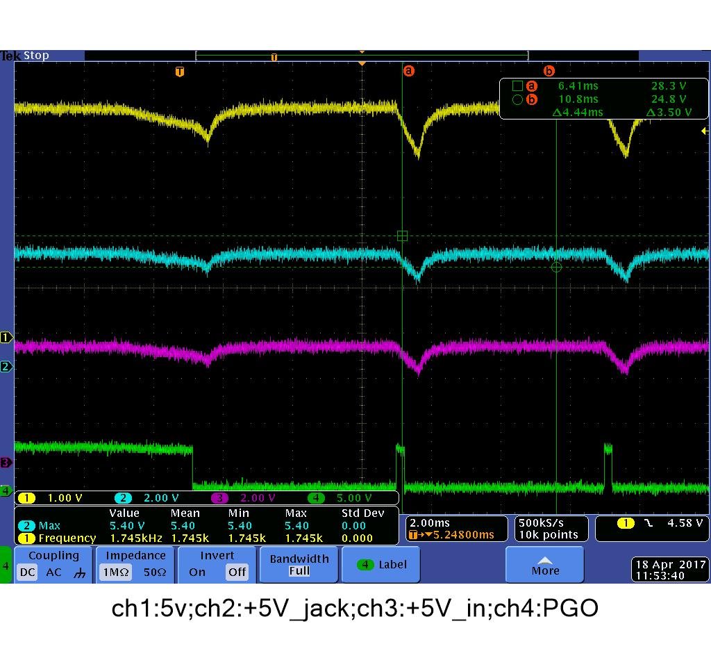
    In my circuit there is a 5V jack input supplying my system through a TPS25944A. The PGOOD signal is used to disable an auxiliary 5V input. I have a problem with the following sequence:
    1)apply 5V auxilary
    2)apply 5V jack
    => PGOOD is asserted
    3)remove 5V jack
    From this point, the circuit oscillates like this at 6.5ms period:
    1)5V decreases down to around 4.4V
    2)PGOOD falls low
    3)auxiliary supply turns ON
    4)5V goes back to 5V
    6)after ~4ms, PGOOD goes high and the cycle continues
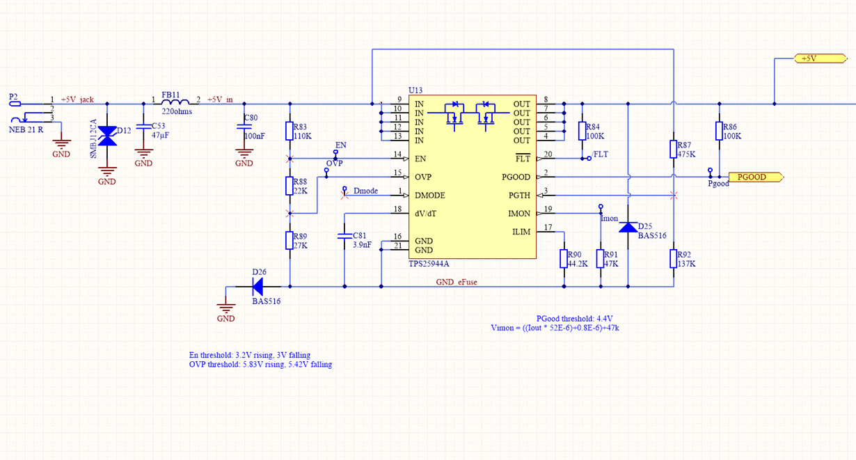
    remark: PGTH is sensing 5V jack input with 137K and 475K resistor network
    On the input, I have a PI filter with 47µF, ferrite bead and 100nF, but I don't see why increasing Cin could solve the problem.
  • Hi Jean Bouchat,

    Thanks for reaching out!
    Can you share the test waveforms at the following points during change over from 5V auxiliary to 5V jack and vice-versa
    5V jack supply voltage, input pin VIN voltage of TPS25944A connected to 5V jack and output voltage.
    It would be helpful if you share the schematic also.

    Thanks
    Rakesh
  • Hello Rakesh,

    I have attached the scope capture and schematic.

    Perhaps, the solution could be to set PGOOD threshold lower than under-voltage threshold? In this case, the TPS25944A will stop before de-asserting PGOOD and therefor not reverse conduct anymore.

  • Hi Jean Bouchat,

    Thanks for the test waveform and schematic.
    From the test result, it is clear that the device U13 is not switching OFF for input power failure. The reason is "When the device is in ON state and the +5V jack is disconnected, the output hold up capacitor at +5V feeds the capacitor at the input node +5V_in. This charging current from +5V to +5V_in should result in more than 10mV reverse voltage drop across the device i.e., 0.25A spike current should flow from +5V to +5V_in. Then, the internal reverse comparator acts and switches OFF the device."
    If input capacitance at +5V_in is not enough, it may not result in >0.25A reverse current and the device remains in ON position.
    Please check with higher value of capacitance at C80 and let me know.
    Revert back if the above explanation is not clear.

    Best Regards,
    Rakesh
  • Hello,
    I added 100µF in // with C80 and it doesn't solve the problem.
    I also tried to chnage R92 to 220K (PGTH ~2.9V) and it solves the problem. The also drawback is that the PGOOD can not be used anymore to validate that the PSU is in the correct range.
  • Hi Jean Bouchat,

    Changing R92 to 220K will result in larger voltage deviation at output because the change over from main source to auxiliary source only happens when output voltage drops below 2.9V. Is this acceptable?
    Let me check the other ways to overcome this issue.

    Best Regards,
    Rakesh
  • Hi Jean Bouchat,

    Can you share the full schematic.
    If it is confidential, please send through email.

    Best Regards,
    Rakesh
  • Hi Jean Bouchat,
    Can you share rest of the circuit to check what best we can do?
    How much tolerance is accepted on +5V bus? Is +5V stepped down to 3.3V in the down stream.

    Best Regards,
    Rakesh