This thread has been locked.

If you have a related question, please click the "Ask a related question" button in the top right corner. The newly created question will be automatically linked to this question.

TPS2115A: Is a floating or 0V input supported?

Part Number: TPS2115A
Other Parts Discussed in Thread: TPS2115, TPS2113A

Hello!

We want to use the TPS2115A in our design.
The power multiplexer will be used as an alternative to an OR-ed diode circuit to enable either board supply via USB or an external 5V auxiliary supply. The board features a LP38692SD-3.3 regulator, that generates the 3.3V voltage required by the logic of the board.
Currently I'm not sure if this device is the best choice. The diode solution cannot be used, as the USB voltage might drop down to 3.9V taken into account the cable drop, the upstream/downstream drop and the VBUS tolerances. If considering the voltage drop of the diode and the dropdown voltage (up to 1V) of the LP38692SD-3.3/NOPB, the board wont operate correctly under a worst case szenario.

It might happen that one of the power inputs (USB or 5V auxiliary) is not connected at all. This means, that one input on the TPS2115A is 0V. The datasheet states in the pin description that the input voltage needs to be higher than UVLO on the inputs. Well, we can't comply with this requirement. Nevertheless, one input will be at least at a voltage of 3.9V, so supplying the TPS2115A is accomplished.
Do you think this will work without any issues?
What will happen at the output, when we would switch to the (floating, 0V) input (the other input is still >3.9V)?

What about reverse leakage current and cross-conducting? As one input is connected to USB, it must be ensured under all circumstances, that no current is feeded back into VBUS, when switched from IN1 (USB) to IN2 (5V auxiliary) and vice versa. Is it ensured, that if no load capacitance is at the output, that the output voltage will shortly drop to 0V? If you look in the datasheet of the TPS2115A it is not clearly, but in figure 4 in the datasheet of TPS2115 (should be similar to the A version), it seems that the voltage does not completely fall down to 0V.

Which device is recommended for new design TPS2115 or TPS2115A?

Regards,
Thomas


  • Hi Thomas,

    Only one input needs to be powered >2.8V, so it is okay if the other supply drops down to 0V. If you are looking for a solution which automatically selects the highest input voltage to power the output, then the TPS2113A is a good choice.

    When the device switches between its two channels, it never has both FETs on, so there is never a risk for current flowing from one supply to the other. While this is a safe way to switch supplies, it does leave the output unpowered for a very short amount of time. If there is no output capacitance, then it will be difficult for either device to prevent the voltage from dropping during this time unless the load is very light.

    Also, when selecting between the TPS2115 and the TPS2115A, the TPS2115A is recommended. For more information on the differences, please see the E2E post below: e2e.ti.com/.../26895

    Thanks,

    Alek Kaknevicius

  • Hello Alek!

    Thanks for your input!!!

    Where is the relevant difference between TPS2113A and TPS2115A? Both can select the highest input voltage source. They should be nearly the same, except the truth table. TPS2115A is about 20% cheaper than TPS2113A, at least at our local distributor.

    Regards,

    Theomas

  • Hi Thomas,

    The TPS2115A has two enable pins (D0 and D1) that can configure the device for manual or automatic switching. The automatic switching happens when one of the supplies is greater than the other supply.

    The TPS2113A only has one enable, and instead of a second enable it has a sense pin that can be configured to select the IN1 voltage threshold where the device switches from IN1 to IN2.

    If the logic of the TPS2115A works for your application and the sense pin is not needed, then either device can work.

    Thanks,

    Alek Kaknevicius

  • Hello!

    I bought the TPS2115A EVM-581 in the meantime, but still have questions.

    What is tPLH2 and tPHL2 in the datasheet? Isn't this parameter a contradiction to the transition time tr?

    Why is transition from IN1 to IN2 much faster than from IN2 to IN1? Whereby this is not true for all input voltages, see the measurements below.

    My setup:
    - J4, J3, J1 are not installed --> the eval board is configured for manual switching
    - J2 is configured as 1k pulldown at D1, as J4 is not installed J2 does not operate as divider.
    - D1 (TP3) is connected to a push button that is connected to IN1 --> is used to switch between IN1 and IN2
    - J8, J7, J6 not installed, only 10µF on output
    - The output of the evalboard is connected to the LP38692SDK 3.3V eval board (additional 10uF input capacitor) with a 8R load (~400mA)

    The mentioned testpoints reference to the http://www.ti.com/lit/ug/sluu409/sluu409.pdf

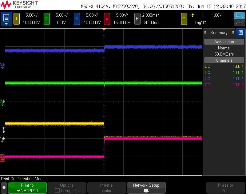
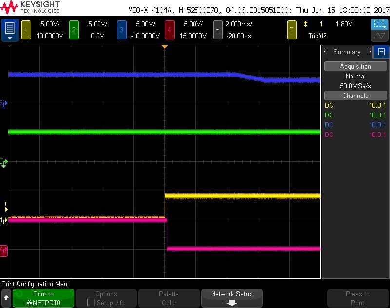
    yellow: TP3, D1 input
    green: TP7, IN2 voltage
    blue: TP2, output voltage of the TPS2115A
    red: STAT pin

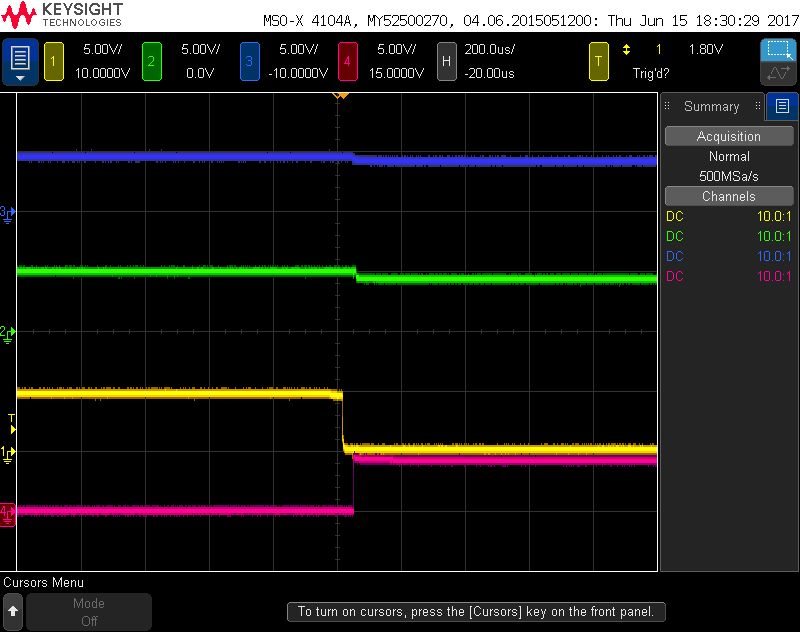
    Picture 1:
    Input voltage on IN1 and IN2 are nearly the same. There is small voltage drop on IN2 due to the small cables used to connect to the power supply. Switching from IN1 to IN2 is pretty fast, about 50µs.

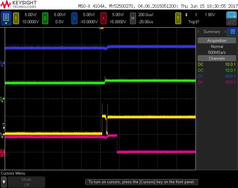
    Picture 2:
    Input voltage on IN1 and IN2 are nearly the same. Switching from IN2 to IN1 is pretty fast, about 50µs. But the STAT signals changes some µs later. However, shouldn't be a great issue, even if in picture 1 the STAT transition is synchronized with the out transition.


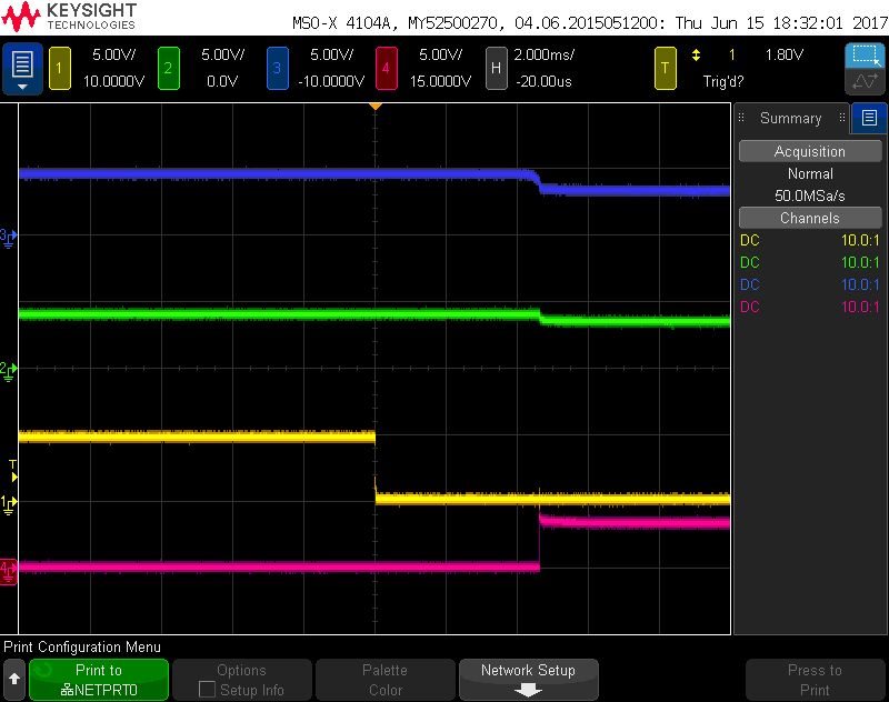
    Picture 3:
    Input voltage IN1 is about 800mV larger than IN2. Switching from IN1 to IN2 takes nearly 3ms. This is indicated by the blue and red signals. Why is the transition in this case as long???

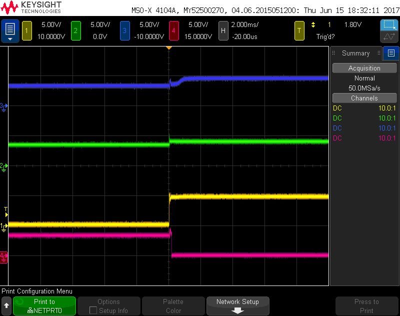
    Picture 4:
    Input voltage IN1 is about 800mV larger than IN2. Switching from IN2 to IN1 takes a few 100µs.

    Picture 5:
    Input voltage IN1 is about 800mV lower than IN2 (so the opposite to picture 3 and 4). Switching from IN1 to IN2 takes just a few µs.

    Picture 6:
    Input voltage IN1 is about 800mV lower than IN2 (so the opposite to picture 3 and 4). Switching from IN1 to IN2 takes about a few ms, seen in the blue signal. However the STAT signal changes immediately. Compare picture 3... Why is there such a big difference between the transistion of the STAT signal?

    Doing all these measurements, what is tPLH2 and tPHL2? I don't get it. Is this only relevant, if IN1 and IN2 are not equal? Why is switching from IN1 to IN2 much slower than from IN2 to IN1??

    Why is this all relevant...
    Imagine the following situation: The electronic should be powered by two different sources, either by an external 5V power supply or via USB. The external power supply is connected to IN1. The USB VBUS is connected to IN2. If both sources are connected, the board is powered by IN1 (the external power supply). If I disconnect the external power supply, there occurs a IN1 to IN2 transition. As this transition takes several ms, the output drops several volts because I can't add 1F ;-)  --> the board resets.
    Currently I try to figure out why this happens. D1 is directly connected to IN1, with a 1k pull-down. So if the external power supply is disconnected and the input voltage IN1 is dropping, the voltage at D1 is dropping as well, till D1 goes below input low level and the TPS2115A switches to IN2. Unfortunately the transition takes a few ms.
    Do you think the problem is the current D1 connection? Should there be used a low voltage detector that is switching D1?

    I did some testing with the automatic mode as well. The output is ringing and I have large ripple on it, if IN1 and IN2 are nearly the same.


    Regards

    Thomas

  • Hi Thomas,

    Timing is described in figure 1, and t_PLH2 and t_PHL2 can be seen as "delay times" while t_R is the "rise time" when the output first comes up. The total turn on time for each channel would be the t_PLH value + the rise time value. The t_t parameter is the rise time when the device is transitioning from one supply to another, and it does not take into account the t_PLH value when switching between supplies.

    The transition from IN1 to IN2 is much faster than the transition from IN2 to IN1 because IN2 is meant to be a backup supply and IN1 is the priority. For example, if a USB cable was your priority supply and a backup battery was your secondary supply, then you would want the transition from USB to battery to be faster since the USB supply is being disconnected. Since the battery is there the whole time, there is no rush to transition back to the USB supply when it is reconnected.

    During all of these transitions, does the output drop low and stay low for ms before the switchover? When the device is switching between IN1 and IN2, if the output voltage is greater than IN2, then the device will not turn on until the output is lower than IN2. That is likely why the IN1>IN2 cases are taking so long to switch over, the device is waiting for the output to be lower than IN2 and the t_PHL1 values are in the ms range.

    Thanks,

    Alek Kaknevicius