This thread has been locked.

If you have a related question, please click the "Ask a related question" button in the top right corner. The newly created question will be automatically linked to this question.

TPS22915: Body diode between VOUT and VIN; ON pin leakage to VIN

Part Number: TPS22915
Other Parts Discussed in Thread: TPS22914

Hello,

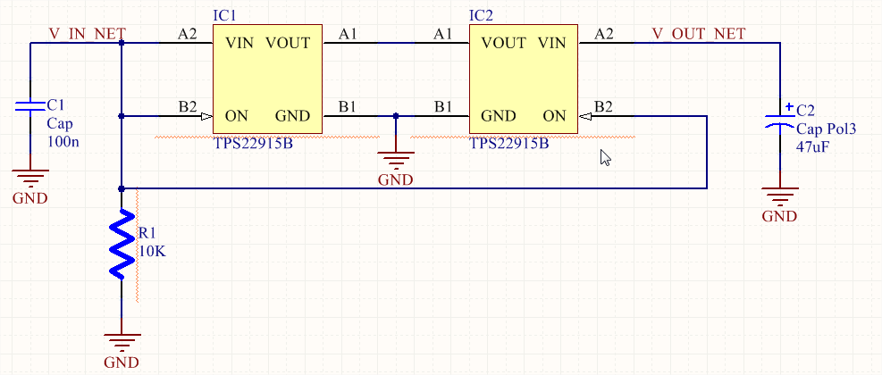
I have a circuit that is designed to isolate the V_IN_NET from any voltage on V_OUT_NET. Vout may be any voltage between 0 to 5V.

Vin has two states;

  • Vin is unpowered, 0V, I want Vin to be isolated from Vout. Any voltage at Vout should not appear at Vin.
  • Vin is powered, 5V, I want a low loss path to Vout.

When Vin transitions from unpowered to powered the operation that occurs is:

  1. IC1 sees VIN=5V, ON = 5V. IC2 ON =5V (but I assume the device isn't being powered as VIN = 0V)
  2. N-fet conducts between VIN and VOUT of IC1 which supplies VOUT of IC2.
  3. The body diode between VOUT and VIN of IC2 brings up VIN of IC2.
  4. IC2 is now powered, and N-fet conducts.

Question:

  • Is there a path where in the case of IC2 VIN can be powered through the ON pin via a body bias diode, ESD diode?
  • Is using the body diode between VOUT and VIN of IC2 a valid use case?

Best regards,

William

  • Hi William,

    Thanks for reaching out! To answer your questions:

    Is there a path where in the case of IC2 VIN can be powered through the ON pin via a body bias diode, ESD diode?

    • Internally, VIN and ON are not coupled, so the ON pin voltage will not be affected by the application of VIN.

    Is using the body diode between VOUT and VIN of IC2 a valid use case?

    • This is not recommended for DC conditions, but for powering VIN to turn the device on, this is a valid use case.

    Thanks,

    Alek Kaknevicius

  • Thanks for the reply Alek,

    I would like to follow up with further questions:

    • I'm surprised to hear there is no internal coupling between Vin and ON pin. I found that the TPS22915 datasheet specifies a maximum input leakage current at the ON pin of 0.1uA when VIN =5.5V. If there is no coupling then why is there a leakage current. Also, wouldn't there be a coupling from ON pin to a reference pin for ESD protection?

    • Could you clarify which scenario is not recommended for the DC condition? I am assuming the scenario where V_OUT_NET is supplied through IC2 body diode to the load and the Nfet is not ON ( VON = 0V). Is this because the body diode is simply not rated for this scenario? Are you saying that using the body diode to turn on IC2, then turn on IC2 load switch, and bypass current away from the body diode to the load switch is a valid use case?

    I had a few new questions related to this circuit:
    • What is the value of Rpd and Ron when VON =0V, VIN = 0 to 1.05V? I assume Rpd and Ron are both high impedance range (>1Mohm).

    • What will be the value of Rpd and Ron when VON = 5V, and VIN is gradually set from 0V to 5V? Will the pull down turn be enabled first or is it not enabled, or does the load switch enable without the pull down activating? The datasheet shows that VON can be 5V, for a VIN between 1.05V to 5.5V. The reason is that I am concerned that IC2 load discharge will be enabled, thus discharging IC1 VOUT, before IC2 is powered via it's body diode to activate its load switch.

    Best regards,
    William
  • Hi William,

    Please find my responses below:

    • The ON pin leakage is specified at VIN=5.5V, but it should not have a strong dependency on the VIN voltage. A voltage on the ON pin will not couple to VIN, and the ESD diodes are relative to ground.
    • The scenario that is not recommended for DC conditions is when the device is off and VOUT>VIN. This will cause the device to pass current through the body diode for a long period of time and we do not characterize the maximum current allowed for the body diode. Using VOUT to power VIN when ON is pulled high is a valid use case.
    • When VON =0V and VIN = 0 to 1.05V, the Rpd resistance is "unknown". The device may power up and enable the QOD resistance, or it could be partially on, or it could be completely off. It is difficult to determine and not guaranteed. That being said, Ron will be high impedance during this time.
    • What will be the value of Rpd and Ron when VON = 5V, and VIN is gradually set from 0V to 5V? Again, this is unknown since for a brief period of time the QOD resistance may be enabled.

    Some suggestions for your circuit:

    • The TPS22914 is the TPS22915 without the Rpd resistance. If the Rpd resistance is not desired, have you considered using two TPS22914 devices instead? Another approach would be replacing one of the TPS22915 devices with a TPS22914.
    • We have load switches with reverse current blocking integrated. The TPS22913C is a similar device with reverse current blocking integrated, so when the device is turned off, current will not be able to pass through from VOUT to VIN if VOUT>VIN.

    Thanks,

    Alek Kaknevicius