This thread has been locked.

If you have a related question, please click the "Ask a related question" button in the top right corner. The newly created question will be automatically linked to this question.

TPS259230-41EVM: TPS259230DRCR

Part Number: TPS259230-41EVM

Hi All,

  • Is there any tool support (webench etc.) for simulating TPS259230DRCR  part ?
  • In the block diagram for the part I see the ILIM block diagram , can anyone please help me to relate the transfer function to this block diagram , meaning thereby how is this transfer function being accomplished through this block diagram given that the ILIM bias current is 10u amp but I see in transfer function RLIM being multiplied by 30u amp
  • What does the Vopen ILIM below indicate ?

  • Is the 6v being used internally output of charge pump ?
  • What is the threshold input voltage at which the  output clamping to 6.1v starts?

  • Hi Siddharth,

    The PSpice model is available at www.ti.com/.../toolssoftware for simulation use

    The equation is derived from the device characterization data to fit the large data points. Are you planning to model the device? Please use device PSpice model.

    When RILIM is open, the internal circuit limits the pin voltage to 3.1V (typ)

    Yes, 6V is generated internally from charge pump circuit

    Depending on operating temparature, the Vovc can be anywhere between 5.5V to 6.75V with typical value 6.1V. So, the device may clamp starting from 5.5V

    Let me know if you need more information.

    Best Regards
    Rakesh
  • thanks for the reply,

    " When RILIM is open, the internal circuit limits the pin voltage to 3.1V (typ) " - on which pin is the 3.1v getting generated?

    5.5v is in the operating range so i am not sure if it should clamp to 6.1v ? Can you please let me know the clamping voltage at 25 Deg C?
  • Hi Siddharth,

    It is on pin 10 "ILIM" of the device

    The input and output pins can handle voltages up to 20V. What voltage your downstream circuitry can tolerate to? Can you provide more details on your application use case. 

    The typical clamping voltage at 25C is 6.1V as per below graph

    Regards

    Rakesh

  • thanks i meant to ask at what voltage does the part start clamping to 6.1v at 25 deg C?
  • Hi Siddharth,

    The device starts clamping when the input voltage exceeds 6.1V. Please refer test waveform Figure 26 in the datasheet for device response during input transient over voltage.

    Regards,
    Rakesh

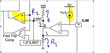
  • As per the datasheet table say at RLIM=150K the voltage at ILIM pin will be 1.5v which should re-appear at pin 1 I suppose as per below marking. R1 as per table computations comes out to be close to 0.3 ohm , is that right?


    Is R2 a passive component or an active device represented as a resistor? Any typical values for the same


    The highlighted Comparator is current comparator or comparing the voltages marked as ILIMIT ?

  • Hi Siddharth,

    The amplifier at ILIM controls the current through R1&R2 to get same voltage 1.5V at pin1. This in-turn sets voltage at node marked as ILIMIT.

    Can you let me know for what purpose you need internal details and what are you trying to achieve? I need to check whether we can share any further information

    Best Regards,
    Rakesh
  • Also please note-the block diagram is an equivalent functional representation, the actual implementation uses active components with compensation techniques based on device operating conditions.

    Regards
    Rakesh
  • please check my mail for further details.