Other Parts Discussed in Thread: TPS22990,
Hi all,
I have a problem in using TI's TPS22966DPUT.
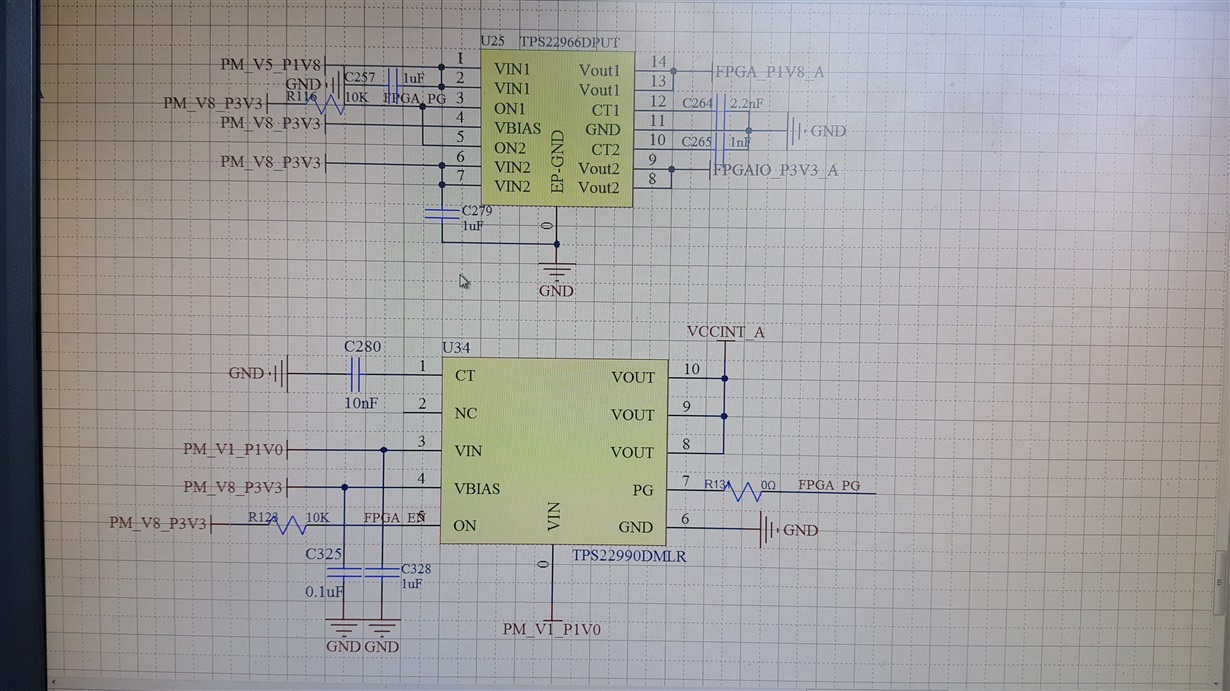
The VCCINT_A is controlled by TPS22990, and the control signal is FPGA_EN. After starting up, FPGA_EN is pulled high in the start-up process, and then the software can be pulled down and maintained by the software.In the process of VCCINT_A, the FPGA_PG also continues to lower, ensuring that the load switch of TPS22966DPUT is in a closed state.
When necessary, pull up FPGA_EN,after connecting VCCINT_A, FPGA_PG output high , 3.3V and 1.8V load switch on.
The problem is described as below.
TPS22990 and TPS22966DPUT are the 1.0V VCCINT cores in the load switch control system, 3.3V IO and 1.8v VCCAUX, and the normal state is closed and opened when needed.
when low temperature test, when the temperature dropped below 0℃, there will be additional power consumption of about 1 w, through practical test, a preliminary confirmation for load switch in low temperature or resistance smaller 200 ohms (room temperature) consume a large amount of electric current.
We have done the following experiments.
1、After starting up, the load switch is maintained as the connection state, and there is no extra large current in the range of -40~+ 85.
2、After starting up, pull down the load switch to keep it off, and the low temperature to 0℃ (exactly 8 ℃) can cause a large current.For 3.3 V IO mouth the cause of the current flow backward, the actual products while the load switch for the off state, still there will be a 2.6 V voltage output end, extra large current appear later, our actual test IO voltage of 3.3 V to 3.3 V, 1.0 V VCCINT decreased from 0.04 V to 0.016 V.This is the reason why we have preliminarily judged that the load switch drain path consumes current.
In the search for the problem, we did the following experiment.
The load switch device is removed without a large current phenomenon, and the problem of load switch is preliminarily suspected.
In the case of the load switch disconnecting, the input and output USES 0 ohms short, and there is no large current phenomenon.
Take the TPS22990 separately or take the TPS22966DPUT separately. There is no extra large current.
I hope you can give me some advices.
1. Is there obvious or potential problems with this circuit that lead to this phenomenon.
2. Whether the device itself will be opened at 0℃ with the outlet opening.


