Hi
I have a few questions related design I need check based on TMS320DM8148CCYEA0.
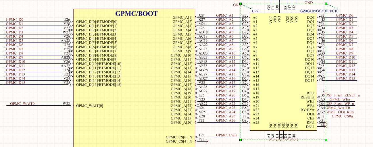
1. Do you have recommended Flash devices list? I use S29GL01GS10DHI010, is it O.K?
2.Can you review the address connectivity at the attached design?
I think GPMC_A1-19 conform MUX1 at table 4.2.
But I don't see A20-23,26 connectivity for MUX1.
At the design I see GPMC_A22(DSP) is routed to AB27 which is GPMC_A22(DSP) at MUX0, is it O.K?
3. At the design BTMODE[4:0]=11011 (First is MUX0), but I think BTMODE[4:0] should be 10001 as first option is MUX1, yes?
Thanks!!!