This thread has been locked.

If you have a related question, please click the "Ask a related question" button in the top right corner. The newly created question will be automatically linked to this question.

66AK2G12: Bring up issue - undesired value of BOOTCFG_DEVSTAT

Part Number: 66AK2G12
Other Parts Discussed in Thread: TPS65400

Hi K2G team,

My customer is nearing production with their K2G project, and they have an urgent board bring up issue:

"I just received my new board. This board is based on the design of K2G ICE board which has single DDR3L chip. My last board is based on K2G EVM it doesn’t have this issue.

After boot up the board and connected to DSP core(C66x) through JTAG. The reading of BOOTCFG_DEVSTAT Register is 0x005EFEBB which is not the desired values.

The bit of NODDR is 1. This disables EMIF and cannot access DDR3L.

The 4-bit LSB of BOOTMODE should be zeros. We have pulldown resistors, 4.7Kohms for those four pins. They should be 0000b(SLEEP mode for using JTAG) but it shows 1101b.

The LENDIAN is 0. The device endian mode is Big endian instead of desired little endian.

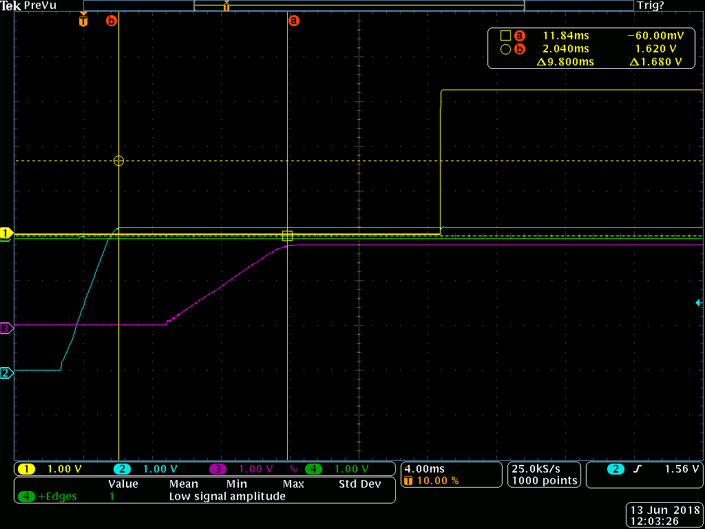
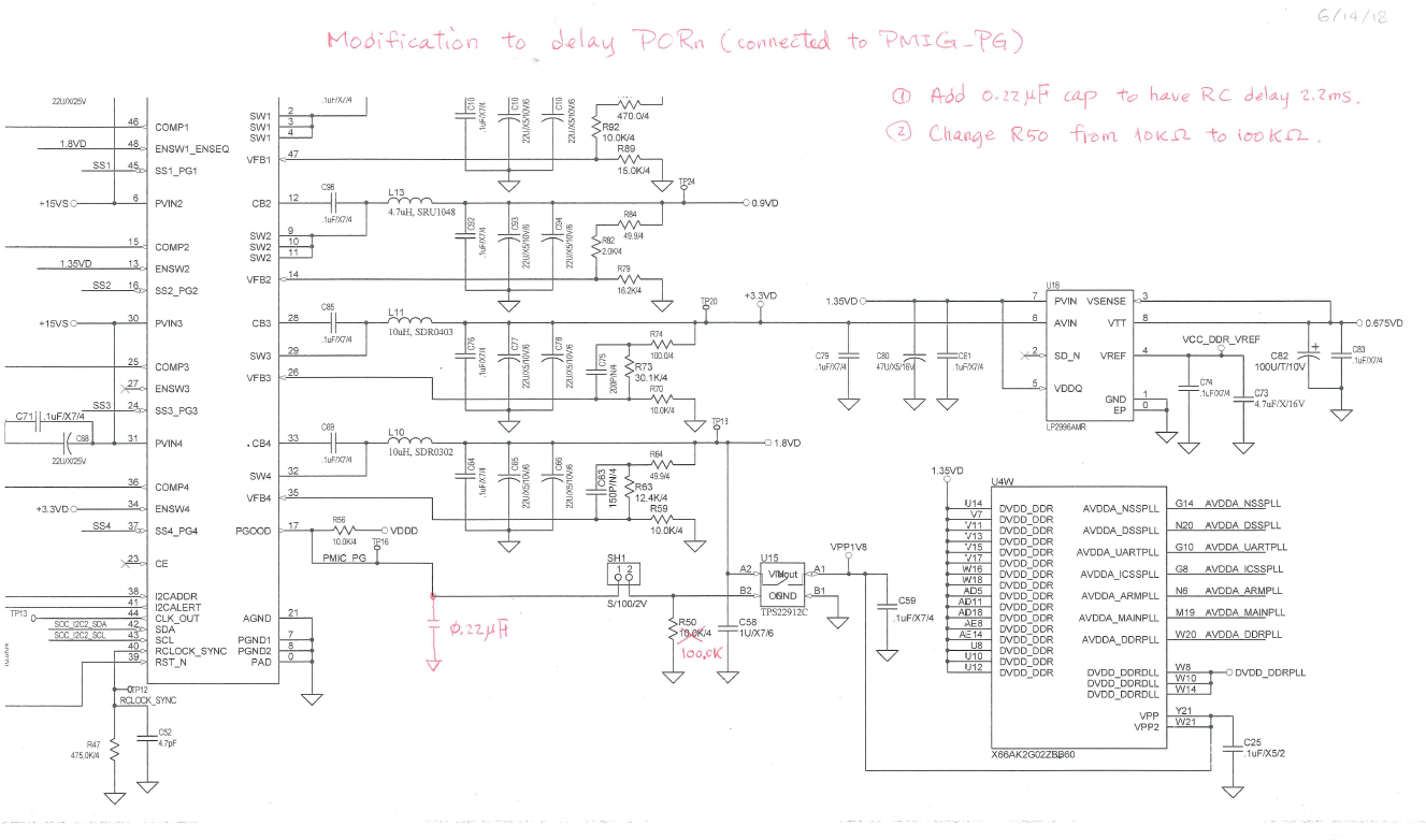
I am going to check PORn and bootmode pins during power up sequence, but can you help point me in the right direction to troubleshoot the undesired value of BOOTCFG_DEVSTAT .


Q1: The bit of NODDR is READ only according to K2G TRM. The pin of NODDR is unconnected in our hardware. Is there any way I can change it to 0?


5.1.4.3 BOOTCFG_DEVSTAT Register (Offset = 20h) [reset = 1h]

BOOTCFG_DEVSTAT is shown in Figure 5-8 and described in Table 5-33.

Indicates device bootstrap selection upon a power-on reset by PORn or RESETFULLn. The default value

of this register is determined by the bootstrap pins. Once set, these bits remain set until a power-on reset.


Q2: Which pin is the LENDIAN bootmode pin? I cannot find it in TRM.


5.1.4.90 BOOTCFG_SYSENDSTAT Register (Offset = 710h) [reset = 0h]

BOOTCFG_SYSENDSTAT is shown in Figure 5-95 and described in Table 5-294.

This register provides a way for reading the system endianness in an endian-neutral way from A15 core.

This register captures the LENDIAN bootmode pin. The value is latched on the rising edge of PORn or

RESETFULLn"

Thanks,

Brian

  • more information here. See below for waveforms of their startup sequence.

    The Ch2(blue color) is 3.3V for K2G’s DVDD33.

    The Ch3(pink color) is 1.8V for K2G’s DVDD18, PLLs.

    The Ch1(yellow color) is PORn signal. This is from PMIC TI’s TPS65400 PGOOD pin. It aligned with K2G’s CVDD (not shown on attached picture)

    The Ch4(green color) is the BOOTMODE03 which is low on the rising edge of PORn. Actually, it’s low all the time as you can see in the picture. But the BOOTMODE03 in BOOTCFG_DEVSTAT register is HIGH. I just use one of BOOTMODE pins to be an example to show you why the BOOTCFG_DEVSTAT is not what I see on the waveforms of the BOOTMODE signals.

    Thanks,

    Brian

  • Hi Brian,

    You mentioned that this design was based on the K2G ICE but that you are using the PMIC. Can you provide some additional detail on the design?  In you statement above you said the PORn is aligned with the CVDD. What is the delay between CVDD and PORn? How are you clocking the part? When is the clock present?

    Regards, Bill

  • Bill,

    Basically they started with the K2G ICE files and adjusted a few things, like the power supply. Here is latest from customer answering your questions, plus followup questions:

    We have done some measurements and find the working fix. But we have the question below.

    PORn(connected to PMIC PGOOD) is deserted right after CVDD(0.9V) ramps up. The delay between CVDD and PORn is very small.

    From our SYSOSC clock measurements, the SYSOSC_IN is not ready before PORn is deserted. The issue of incorrect BOOTMODE values is resolved after we delay PORn more than 2ms after SYSOSC_IN is stable.

    Please see attached picture for power up sequence from the following power/clocks.
    The Ch1(yellow color) is K2G’s SYSOSC_OUT.
    The Ch2(blue color) is 1.8V for K2G’s DVDD18, PLLs.
    The Ch3(pink color) is K2G’s SYSOSC_IN.
    The Ch4(green color) is CVDD (0.9V).

    SYSCLKSEL, not shown in the picture, is always LOW.


    Refer to K2G data sheet Table 4.1, the corresponding power supply for both SYSOSC_IN and SYSOSC_OUT is DVDD18 (1.8V). But form the attached picture, the SYSOSC_IN and SYSOSC_OUT start oscillating after CVDD(0.9V) ramps up. This is more than 10ms after DVDD18 ramps up. Is the data sheet wrong about the corresponding power supply?

    Thanks,
    Brian
  • Hi Brian,
    The HF oscillator uses the DVDD18 for the IO supply but the control logic for the entire part is based on CVDD. Since the control signals for the oscillator are not stable without CVDD, the oscillator isn't going to start until that supply is present. The power sequencing defined in Figure 5-3 must be met for the device to boot correctly. Although there is no timing requirement shown it's implied that the PORz must remain low until all power supplies are stable. The timing is specified from when the oscillator is stable to the release of PORz. This is needed to allow the device to properly clock the reset to all the internal IPs. As you found, once you meet the 2ms delay between the clock and the rising edge of the PORz, the device boots correctly.
    Regards, Bill
  • Bill,

    Q1: My customer has modified their schematic a little to add a delay on the PORn signal. Can you let us know if this method will be sufficient?

    Q2: During the measurement of power up sequence I noticed the amplitude of SYSOSC_IN is kind of small as you can see in the below picture.The Ch1(yellow color) is K2G’s SYSOSC_OUT. It swings between 0 to 1.8V. But Ch3(pink color),  K2G’s  SYSOSC_IN, only swings 0.45V to 1.3V.

    Based on the datasheet, the VIL=0.35*1.8V=0.63V; VIH=0.35*1.8V=1.17V. we only have less than 0.2V margin for both VIL and VIH. Is there any concern about it? Do we need to improve it? If so, how? Could this be a load capacitance issue? The crystal we use has CL=12pF. The Cf1 and Cf2 (refer to datasheet Table 5.3) on our design is 22pF. If use  Figure 5-16. Load capacitance equation in the data sheet. The Cf1 and Cf2 should be 24pF.


    I also notice the old K2G datasheet for crystal shunt capacitance is TBD but the specification in new datasheet is max. 4pF. The crystal we use is ABM8AIG-25.000MHZ-12-2Z-T3. It was chose before the spec was available. Its shunt capacitance is max. 7pF. What would happen if shunt capacitance is out of spec?


  • Update, the delay implemented on PORn was effective, that issue is resolved.

    So the remaining question about the crystal remains.

    The requirements for crystal in the latest K2G data sheet is really strict. The crystal we use is ABM8AIG-25.000MHZ-12-2Z-T3. That’s based on the old data sheet. It will not meet the requirement of frequency accuracy which we need to combine frequency tolerance, frequency stability, aging, etc. What will happen if our crystal doesn’t meet frequency accuracy?
    Do you have any good candidates for 25MHz crystal which meets K2G requirements?

    Thanks,
    Brian
  • The frequency accuracy requirement defined in the data manual is based on the RMII Ethernet interface requirement. If RMII is not being used, the accuracy only needs to be 100ppm.

    We only define the crystal requirements and do not recommend specific components. The system designer will need to select the crystal circuit components and validate they perform as expected over all operating conditions expected for their system.

    Early revisions of the data manual were Advanced Information and some of the content may have been incorrect or incomplete. That is the case with the crystal requirements. The oscillator was designed with the expectation that a crystal with less than 4pF would be used. The value for this parameter was TBD while negotiating with the analog design team for a higher value. We determined the maximum shunt capacitance value provided in typical crystal data sheet may not represent actual shunt capacitance of the crystal.

    We reference the following note on each table in the 66AK2G1x data manual that defines crystal circuit requirements.
    *******
    It may be difficult to find a crystal that meets all of the requirements defined in this table when searching commonly available crystal data sheets. Most commonly available crystal data sheets are non-part number specific and publish worst case parameters for all crystal within the family or series. For example, the data sheet may publish a single value for ESR and shunt capacitance which represents the
    worst case value for every part number within the series. However, these values may be much lower for higher frequency crystals within the series.

    The recommended approach is to search non-part number specific data sheets to identify a few candidates that meet your specific system requirements along with the requirements defined in this table. Once a few candidates have been identified, contact the respective crystal manufacture and request part number specific data sheets to validate each crystal specific parameter meets all requirements.
    *******

    This note was added because customers commonly have problems selecting crystals from information provided in data sheets found on the web. These data sheets typically provide worst case values of a wide range of crystals. There is a very good chance the shunt capacitance the 25MHz crystal being used is much lower than 7pF. They should ask Abracon to provide a device specific data sheet for part number ABM8AIG-25.000MHZ-12-2Z-T3.

    Many crystal manufactures offer a service that verifies the crystal circuit implemented in a specific system provides adequate margin of operation. We recommend this approach for any customers that are not comfortable with their selection of crystal and crystal circuit components. A description of this service begins on page 4 of the Abracon ABM8AIG data sheet found on the DigiKey web site.

    Regards,
    Paul