This thread has been locked.

If you have a related question, please click the "Ask a related question" button in the top right corner. The newly created question will be automatically linked to this question.

RTOS/AM5728: PCIe - How to Retrieve EP BAR

Part Number: AM5728
Other Parts Discussed in Thread: SYSBIOS

Tool/software: TI-RTOS

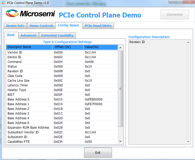
I'm running TIRTOS on AM5728 SOM with a Microsemi Igloo2 FPGA PCIe device plugged into the PCIe slot.  I have a successful linked up and can access the EP vendor and device info.   However, I'm having difficulty with figuring how to access the EP BAR addresses so i can turn on/off the its LEDs.  Base on the Linux device driver for this device, i need to use the BAR0 + LED_OFFSET.  Can I use the same method?  It is so, how can i request the BAR addresses from the FPGA?

Thanks.

  • Hello!

    During enumeration process root complex assigns base addresses to BARs of endpoint, so RC knows those base addresses. However, there is no way for RC to know actual layout of memory or i/o device behind that BAR. In other words, RC should have prior knowledge about layout of EP. After that theses are simple accesses like BARx + OFFSET.

  • Thanks for helping.  I'm new to this; so I've more questions that i hope you could help:  With the layout of i/o device, is using the outbound address as base address and access the i/o possible (I've only one i/o)?  or do  i need to call Pcie_cfgBar() to configure the i/o BARs? if calling Pcie_cfgBar() is the only option, do i use the size of each memory windows to set the barCfg.base with the first one set to zero?  or can i pick an available address location within my RC memory map for those i/o BARs?

  • My I/O vendor provides these information: for BAR0, 0x4_0000 as local to translate to 0x4000_0000. I used 0x4000_0000 in the following code block:

    barCfg.location = pcie_LOCATION_REMOTE;
    barCfg.mode = pcie_EP_MODE;
    barCfg.base = FPGA_BAR0_BASE;
    barCfg.prefetch = pcie_BAR_NON_PREF;
    barCfg.type = pcie_BAR_TYPE32;
    barCfg.memSpace = pcie_BAR_MEM_MEM;
    barCfg.idx = 0;

    if ((retVal = Pcie_cfgBar(handle, &barCfg)) != pcie_RET_OK)
    {
    PCIE_logPrintf ("Failed to configure FPGA BAR0 (%d)\n", (int)retVal);
    exit(1);
    }

    Later on, I requested the type0BarIdx, the results are: raw = 0x4000_0000; but base = 0x0400_0000

    Which one should I use as BAR0 for the i/o? Using the memory browser, it shows the 0x4000_0000 with "-------" to indicate no-read region.

    I'm using the pcie_sample.c as the test driver.
  • Hi,

    In your case, the AM572x is the PCIE RC running TI-RTOS code. The FPGA is the PCIE EP. You have the linked up successfully.

    The data access (R/W) from AM572x side looks like below (I use PCIESS1 here for simplicity):

    • The CPU access (R/W) the the PCIe_SS1 Configuration space address 0x2xxx_xxxx
    • There is outbound translation setup to convert this 0x2xxx_xxxx to PCIE address. The pcie_sample.c code has two outbound regions:
    1. OB region 0 used to access remote EP configuration space offset 0x1000 to 0x1FFC. So if you look at 0x2000_1000 you should be able to access FPGA side configuration space, starting from device id/vendor id. E.g., 0x2000_1010 you should be able to access BAR0 of FPGA.
    2. OB region 1 used to access remote EP memory space offset 0x0100_0000 with 16MB window. So, if you want to access FPGA side data space, you need to look at 0x2100_0000 and onwards. This OB setup the outbound access to 0x7000_0000. It means when you look at 0x2100_0000 on RC side, the PCIE address cross the connection is 0x7000_0000. Then in your FPGA side, you need an inbound mapping of this 0x7000_0000 into some internal memory.

    Given you know that there is a fixed mapping for FPGA side: 0x4_0000 as local to translate to 0x4000_0000.

    What you need to do:

    1. In the RC side for the OB1, you need to change 0x7000_0000 to 0x4_0000
    2. In the RC side you need to do a Pcie_cfgBar() for the remote BAR with barCfg.base = 0x4_0000; From RC side 0x2000_1010 you can cross-check this value.

    What happened is: on RC side, you W/R 0x2100_0000, it translates to 0x4_0000 over the PCIE interface. Then this address is accepted at the FPGA side with BAR matched. Then the FPGA converts the 0x4_0000 into 0x4000_0000. If you know the LED offset, you should be able to access it with 0x2100_0000 + offset (subject to earlier configured 16MB window size).  

    Regards, Eric

  • hi Eric,

    Thanks for the tutorial.  I've a better understanding, but I still can't command the EP to turn the its LEDs on/off.  Maybe, I didn't do step #2 correctly.

    I can't cross check the value on step #2.  A memory view at 0x2000_1010 shows 0x0000_0000.  Should I see 0x40000 at 0x2100_1010?

    For step #1, I changed the PCIE_OB_LO_ADDR_RC from 0x70000000 to 0x40000

    For step #2, i added the following Pcie_cfgBar() right after the pcieWaitLinkUp() an pcieCheckLinkParams(handle).  The call was successful.

      barCfg.location = pcie_LOCATION_REMOTE;
      barCfg.mode     = pcie_EP_MODE;
      barCfg.base     = 0x40000;
      barCfg.prefetch = pcie_BAR_NON_PREF;
      barCfg.type     = pcie_BAR_TYPE32;
      barCfg.memSpace = pcie_BAR_MEM_MEM;
      barCfg.idx      = 0;

      if ((retVal = Pcie_cfgBar(handle, &barCfg)) != pcie_RET_OK)
      {
        PCIE_logPrintf ("Failed to configure FPGA BAR0 (%d)\n", (int)retVal);
        exit(1);
      }

  • Hi,

    Yes, you should see that BAR0 of your FPGA is 0x0004_0000. How many BARs you have on FPGA side? If you have only one BAR (that is BAR0). The code in step 2 looks right but seems the FPGA didn't take it. Is your BAR0 a memory BAR or I/O BAR? WIll below help?

    barCfg.location = pcie_LOCATION_REMOTE;
    barCfg.mode = pcie_EP_MODE;
    barCfg.base = 0x40000;
    barCfg.prefetch = pcie_BAR_NON_PREF;
    barCfg.type = pcie_BAR_TYPE32;
    barCfg.memSpace = pcie_BAR_MEM_IO;
    barCfg.idx = 0;

    if ((retVal = Pcie_cfgBar(handle, &barCfg)) != pcie_RET_OK)
    {
    PCIE_logPrintf ("Failed to configure FPGA BAR0 (%d)\n", (int)retVal);
    exit(1);
    }

    Can you let me know how the 0x2101_1000 to 0x2101_1024 looks like from AM57x side? This should be your FPGA's VENDOR_DEVICE_ID, STATUS_COMMAND, .... BAR0, ... BAR5. If you manually change the 0x2101_1010 through CCS memory window to values like 0x0004_0000 or 0x0004_0001, or 0x0004_0008 or 0x0004_0009 (save the time for debug purpose, w/o change code and reload and run). Will it help?

    Do you have a way to program the BAR register on FPGA side directly (instead of programming it from AM57x remotely)?

    Regards, Eric
  • The EP has 2 BARs (BAR0 maps to 0x4_0000 and BAR1 maps to 0x2_0000) and we have no way to program to EP BAR registers directly.

    0x21xx_xxxx shows all 0xFFFFFFFF

    However, 0x2000_1000 shows:

    0x20001000  11AA11AA 00100000 00000000 00000000 00000000

    0x20001014  00000000  00000000  00000000  00000000 00000000

    0x20001028  00000000  000011AA 00000000 00000000 00000000

    0x2000103C  00000100 00000000 02126160 00000000 00000000

    0x20001050   00817805 02000000 00000000 00000000 00000000

    0x20001064   00000000 00007811 00000000 00000000 00000000

    0x20001078   48038001 00000008 02020010 10008FE1 000B2810

    0x2000108C   01068C41 10110000 00000000 00000000 00000000

    0x200010A0   00000000 00000000 00000000 00000000 00000000

  • hi Eric,
    I found these settings in the .cfg file; what are they for? do i need to change them for my EP? Thanks.
    var peripheralBaseAddrs = [
    { base: 0x4ae00000, size: 0x00100000 }, // PRM
    { base: 0x51000000, size: 0x00800000 }, // pcie_ss1 regs
    { base: 0x51800000, size: 0x01000000 }, // pcie_ss2 regs
    { base: 0x20000000, size: 0x10000000 }, // pcie_ss1 data
    { base: 0x30000000, size: 0x10000000 }, // pcie_ss2 data
  • Hi,

    { base: 0x51000000, size: 0x00800000 }, // pcie_ss1 regs
    { base: 0x51800000, size: 0x01000000 }, // pcie_ss2 regs
    { base: 0x20000000, size: 0x10000000 }, // pcie_ss1 data
    { base: 0x30000000, size: 0x10000000 }, // pcie_ss2 data

    They are PCIE register memory space and data memory space, the SYSBIOS uses those information (starting address and length) to setup MMU, you don't need to change that.

    Regards, Eric
  • Hi,

    So the FPGA side you have two BARs, you mentioned that LED is accessed by BAR0+OFFSET, is this correct? Or it is BAR1+OFFSET? What is the OFFSET value? Typically BAR0 is automatically pointed (hard wired) to the the PCIE configuration space in the PCIE EP side, this is the design of TI PCIE module. I am not sure if the same on the FPGA side.

    From your access of 0x2000_1000, as I saw offset 0x0 value 0x11AA11AA=====> is this your vendor/device id? offset 0x80 showed 02020010 ====> so you got GEN2 speed with 2 lanes, correct?

    I want to try 1) if you can find out the BAR0 mask value (what you setup for the BAR0 mask?) and 2) change the BAR0 address, from the RC side by poking the 0x2000_1010 address.

    For 1) One way to verify if the BAR Mask registers have been set correctly is to write the pattern values into BAR registers and see if the bits have been masked correctly. For example, you have pre-set BAR0 MASK = 0x0000_3FFF. You write BAR0 = 0xFFFF_FFFF; BAR0 should be read as 0xFFFF_C000 because the lower bits of BAR0 have been masked.

    For 2) Try to change BAR0 to 0x0004_0000 or 0x0004_0001, or 0x0004_0008 or 0x0004_0009. Will you see the value reflected in CCS? Or you still see BAR0 = 0?

    Regards, Eric
  • The vendor/device id and GEN2 data are correct based on the information my vendor provided.

    I can set  EP BAR with idx=1 and can see 0x40000 in 0x2000_1011 but not at 0x2000_1010.  However, when i set 0xFFFF_FFFFF to address 0x2000_1010, it changes to 0xFFF0_0000, but set it to 0x4_0000, reset it back to 0x0.

    When i change 0x4_0000 at  0x2000_1011 to 0xFFFFFFFF, CCS refreshes the value to 0xFFFF0000.   If I set it to 0x4_0001 or 0x4_0002/3/4, CCS shows 0x0004_0000

    This is the default BAR mask in pcie_sample.h

    #define PCIE_BAR_MASK        0x0FFFFFFF

    These are the information that my vendor provided to be used with their GUI on WIndows/Linux.  This description on paragraph 2.5.1 in the attached file.

    – Select Window 0 and configure following settings:
    • Size: Select as 1 MB from the drop-down list
    • PCIe BAR: Select as Bar0 from the drop-down list
    • Local Address: Enter values as 0x40000 to translate the BAR0 address space to CoreGPIO
    address (0x4000_0000)
    – Select Window 1 and configure following settings:
    • Size: Select as 64 KB from the drop-down list
    • PCIe BAR: Select as Bar1 from the drop-down list
    • Local Address: Enter values as 0x20000 to translate the BAR1 address space to
    COREAHBLSRAM address (0x2000_0000)

    Microsemi_SmartFusion2_PCIe_Control_Plane_Liberov11p8_Sp1_Tutorial_TU0456_V9.pdf

  • Hi,

    I interpret 0x2000_1011 as 0x2000_1014, because this is 32-bit address and BAR1 is at 0x2000_1014.

    For your trial of writing 0xFFFF_FFFF to BAR0 and got 0xFFF0_0000, this confirmed the BAR size is 0x10_0000. That is 1MB, matched your document excerpt. Similarly, BAR1 is 64KB from your trial. This also matched the document excerpt.

    For a BAR0 mask of 1MB, it masks bit 0-19. So you wrote a 0x4_0000 and got 0x0000_0000. It is expected. I don't understand "Local Address: Enter values as 0x40000 to translate the BAR0 address space to CoreGPIO address (0x4000_0000)" on the FPGA side." Maybe you can check the FPGA vendor for this.

    Some thing we can try on AM57x side,

    1) 

    barCfg.location = pcie_LOCATION_REMOTE;

     barCfg.mode     = pcie_EP_MODE;

     barCfg.base     = 0x40000; =========> change this to 0, as it has no effects

     barCfg.prefetch = pcie_BAR_NON_PREF;

     barCfg.type     = pcie_BAR_TYPE32;

     barCfg.memSpace = pcie_BAR_MEM_MEM;

     barCfg.idx      = 0;

     if ((retVal = Pcie_cfgBar(handle, &barCfg)) != pcie_RET_OK)

     {

       PCIE_logPrintf ("Failed to configure FPGA BAR0 (%d)\n", (int)retVal);

       exit(1);

     }

    2) In the pcie_sample.c, there is a function called pcieRet_e pcieObTransCfg(Pcie_Handle handle, uint32_t obAddrLo, uint32_t obAddrHi, uint8_t region)

    You see there is an additional region configure for RC mode

    if(PcieModeGbl == pcie_RC_MODE)
    {
    /*Configure OB region for remote configuration access space*/
    regionParams.regionDir = PCIE_ATU_REGION_DIR_OUTBOUND;
    regionParams.tlpType = PCIE_TLP_TYPE_CFG;
    regionParams.enableRegion = 1;

    regionParams.lowerBaseAddr = PCIE_WINDOW_CFG_BASE + resSize;
    regionParams.upperBaseAddr = 0; /* only 32 bits needed given data area size */
    regionParams.regionWindowSize = PCIE_WINDOW_CFG_MASK;

    regionParams.lowerTargetAddr = 0U;
    regionParams.upperTargetAddr = 0U;

    if ( (retVal = Pcie_atuRegionConfig(
    handle,
    pcie_LOCATION_LOCAL,
    (uint32_t) 0U,
    &regionParams)) != pcie_RET_OK)
    {
    return retVal;
    }
    }

    Where #define PCIE_WINDOW_CFG_MASK 0x00000FFFU

    This is a configuration translation to access the FPGA side PCIE registers with a 0x1000 window. That is why from AM572x side (0x2000_1000 to 0x2000_2000) you can look into FPGA side BAR0 for 0x1000 memory range (e.g, device/vendor ID, BAR, etc...).

    Please update the PCIE_WINDOW_CFG_MASK to a big number like  0x1F_FFFF (that is 2 MB window). Then from AM57 side, make sure the increase doesn't break your access of FPGA by looking into 0x2000_1000 region. Then try to look at 0x2004_1000 or 0x2004_0000 (just do it via CCS memory window) to see if the FPGA can map this 0x4_0000 address into your GPIO region.

    If still no luck, please try to check the FPGA vendor how to setup the access of BAR0 with address 0x4_0000. If this is a CFG access or MEM access? 

    Regards, Eric

  • hi Eric,

    Using the driver and a demo program from the board vendor, we are able to see the following settings on Windows.   Is it possible to use these information to configure TI RTOS so it can R/W to the FPGA?

    If is possible, could you help with the changes?  Thanks.

  • Hi,

    When you use a PCIE RC with an operating system, like Windows or Linux machine, it worked differently than using the AM572x running RTOS code. The former has OS and does the enumeration, it reads in the BAR0/1 mask of EP and determine the memory address allocated and writes into the BAR0/1 of EP side. When you use the latter, it doesn't have enumeration process and the configuration of both RC and EP side is static.

    In your Windows PC test case, are you able to toggle the LED? How? E.g. accessing 0xFE80_0000 + 0x4_0000 + OFFSET?

    Then you can do the same way in RTOS like Windows PC case:
    1) in the CCS memory view, change the BAR0 of EP (address 0x2000_1010 = 0xFE80_0000).
    2) in the AM572x RC side, when configure the OB translation, use 0xFE80_0000 as the outbound address (instead of 0x0000_0000 or 0x40000 or 0x7000_0000).

    Regards, Eric
  • hi Eric,

    With the completion of step #1 and #2,  I can see BAR0 set to 0xFE80_0000 at 0x2000_1010, and from CCS, I can view and set values at 0xFE80_0000 + <offset>.   However, I still can't  control the LEDs with numerous offsets provided by my FPGA vendor.

    Is there any other ways within CCS that would help me verifying if EP BAR0 is set properly and if there is any outbound address translation going on that could mess up the address mapping?

    Thanks.

  • Hi,

    "....and from CCS, I can view and set values at 0xFE80_0000 + <offset>. However, I still can't control the LEDs with numerous offsets provided by my FPGA vendor"

    From CCS side, if you can R/W the values at 0xFE80_0000 + <offset>. Then on the FPGA side, you need an inbound mapping to translate 0xFE80_0000 into CoreGPIO address (0x4000_0000).

    Regards, Eric