This thread has been locked.

If you have a related question, please click the "Ask a related question" button in the top right corner. The newly created question will be automatically linked to this question.

66AK2G12: K2G PCB Guidlines for QSPI

Part Number: 66AK2G12
Other Parts Discussed in Thread: AM5748

Hi, we are designng a board using 66AK2G12 and we want to implement a QSPI.

I found this answer K2G PCB Guidlines for QSPI (https://e2e.ti.com/support/processors/f/791/t/541174) and tried ti simulate what you suggest.

The problem is that while the 66AK2G12 QSPI_RCLK signal is beautiful the memory CLK input is horrible.

What should I do?

Regards,

Roberto Vigliarolo

  • Hi,

    I am looking into this. Could you share the scopes for both signals QSPI_RCLK & memory CLK input?

    Best Regards,

    Yordan

  • Hi Yorgan,

    thank you for your prompt response.

    I made a simulation as suggested in note 1 on page 50 of SPRSP07E.

    You can see in the attached file the result of this preliminary simulation of the net configuration suggeted in e2e.ti.com/.../541174 and also in SPRS953F page 400 and 401.

    I think the problem is that connecting in the middle of a series terminated line give always give you risk of incorrect clocking that can cause unpredictable behavior.

    Do you any other suggestion?

    Regards,

    Roberto

    P.S.

    Sorry for my double posting: I tought the first massage was not sent.

    QSPI CLK simulation.pdf

  • Hi Roberto,

    There is a more detailed list of routing guidelines in the AM5748 data sheet that you can use as a reference. Check section 7.6.2 for that information. The diagram in that section is very similar to yours minus a source terminating resistor at the K2G. That source terminating resistor can be used to tune the shape of the clock signals at the destinations. This can also be done by changing the resistor values that are closer to the memory. 

    An alternative method would be to include two source terminating resistors as close as possible to the K2G. The second side of one of those resistors would be connected to the memory and the second side of the other resistor would be connected to the RCLK pin. You would need to ensure that the trace to the RCLK pin matches the length needed for the clock to travel to the memory and back.

    Regards, Bill

    http://www.ti.com/lit/ds/symlink/am5749.pdf

  • Hi Bill,

    thank you for your answer.

    The same routing suggestion you mention is also in a document you can find in the product page for 66AK2G12 (66AK2Gx Schematic Checklist (Rev. A) SPRAC54A) section 2.17.

    The problem is that, following that guideline, I cannot achive a reasonable clock waveform for both K2G12 and FLASH memory, as demonstrated with my previosly posted simulation.

    I tried also your last suggestion with lightly QSPI CLK simulation same delay.pdfbetter results but I didn't achieve a sufficently clean clock waveform.

    The reason is that for this method to work the reflection from memory clock input and RTCLK ball should arrive at the same time to achieve a clean signal waweform.

    I tried a simulations using two different values for transmission lines impedance (the impedance of the two separated branches is about double the impedance of initial launch line) and making the delay of the two branches the same (see my attached simulation).

    Of course doing this the RTCLK signal arrives at the same time the memory receive a clock signal.

    I don't see any reason why the clock at RTCLK slould arrive later than that.

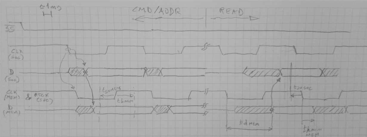
    I have tried a timing diagram, assuming line delays for clk to mem and data to mem of 1 ns, for sake of simple representation, and it seem all is OK (my memory have a clock to data delay of 6 ns MAX and a data hold time from clock of 1.5 ns).

    I am not sure I understand well the read data capture of QSPI in 66AK2G12: section 11.15.4.2.1 of TRM (SPRUHY8I) to me is not very clear.

    So I ask you to check my timing diagram and confirm I understood well the behawhiour of K2G12 logic.

    In case there are still problems I ask you to provide a simulation of the net configuration you suggest in order to see that clock waveform is OK on both RTCLK and memory clk input.
    This simulation is advised for in data sheet on section 4.3.8 note 1.

    Regards,

    Roberto

  • I Bill,

    I forgot to attach the timing diagram.

    Please find it attached here.

    Regards, Roberto

  • Hi Roberto,

    It will take me some time to check the values in your diagram. What is your criteria for declaring a clock signal clean? The shelf caused but reflection is expected. Tuning the resistor values can raise or lower the voltage where the clock signal flattens out due to the reflection. As long as that voltage is above the Vinhmin on the rising edgne and below the Vinlmax on the falling edge the clock should be valid at the memory device.

    Regards, Bill

  • Hi Bill,

    I completely agree with you.

    The problem is my memory, a typical one, has CMOS thresholds (0.3 and 0.7 Vcc) and implementing the circuit suggested by TI and simulating it with nominal values the shelf is in the forbidden range. Of course, applying tolerances due to production, temperature, etc. make things only worse.

    Regards, Roberto

  • Hi Roberto,

    Although it doesn't follow the guidelines I agree that the timing diagram you provided appears to be valid. We haven't tried operating the device with the routing you provided but I don't see any issues once I reviewed the timing for the part. I'm sorry it took so long to get back to you on this issue. 

    Regards, Bill