This thread has been locked.

If you have a related question, please click the "Ask a related question" button in the top right corner. The newly created question will be automatically linked to this question.

AN SCAA880: PLL not locking

Other Parts Discussed in Thread: CDCE913

Hello all!

I'm trying to implement Application Note SCAA088 to generate a master clock from a I2S source (from a CD player). But I'm having some troubles getting it to work as the PLL is not locking (and thus the output is running freely and not in sink with the input source). This is my schematic:

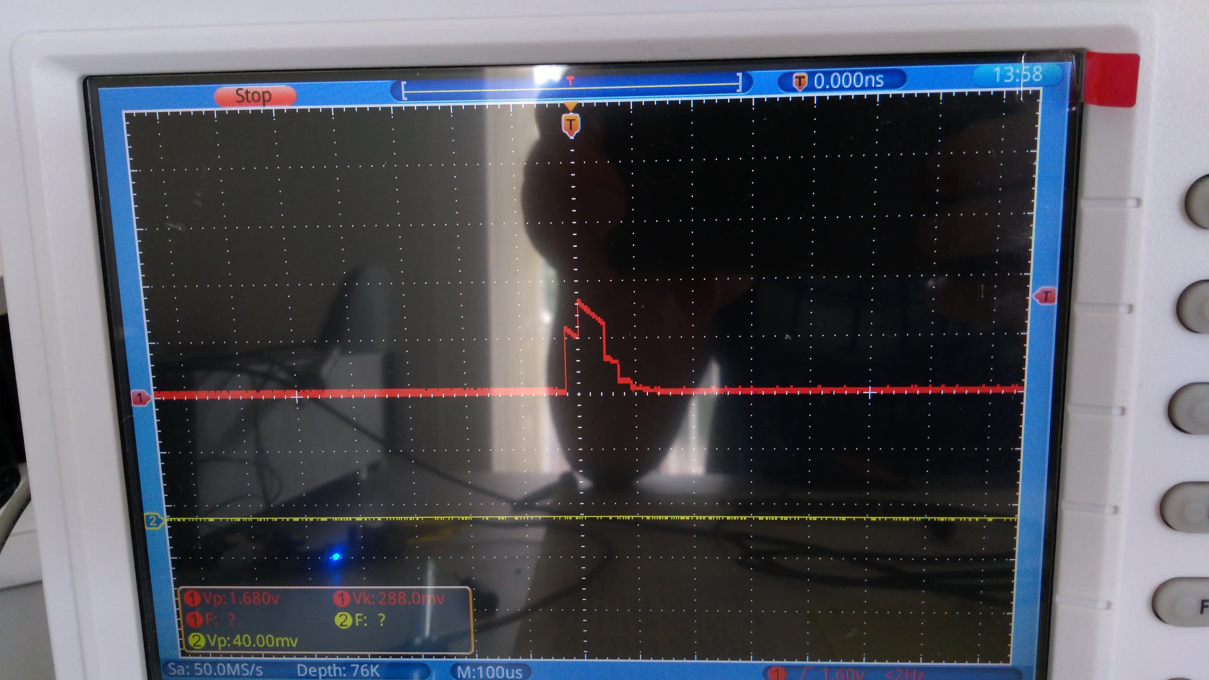
I've set the output dividers properly to the desired values (Y1 outputs a clock of 44.1KHz, Y2 has half the crystal frequency) and the CDCE913 is configured to operate in VCXO mode. But it seems like the signal from the phase comparator is not arriving properly at the CDCE913. (it's flat zero). when removing the RC-filter, this is what I see on the oscilloscope:

Still no difference in the locking of the PLL however... Does anyone have some pointers for my to try?

  • Hi Niek,

    Can you share your configuration file and the datasheet for your crystal?

    Kind regards,
    Lane
  • Hi Lane!

    With the configuration file you mean the register settings written to the CDCE913? (i'm writing to it using a microcontroller)

    The crystal used is a ABL-11.2896MHz-B4Y. I've attached the datasheet.

    Thanks for looking into this!

    Regards,

    Niek ten Brinke

    ABL-10083.pdf

  • Hi Lane!

    Here are the register settings that are written to the CDCE913:

    Forgot to say, but we removed the capacitors from the board (and set the internal caps to 20pF as you can read above)

  • Niek,

    I'm used to working with PLLs at much higher frequency and with a charge pump instead of a voltage phase detector, but still I think that your schematic seems suspicious to me. I'm looking at figure 5 in the application note and comparing it to what you have.

    1. I know in the op amp they have the output of the op amp shorted to the input, but does this make sense? I suspect this is an error. Maybe the intention was that the output voltage was near 1.8 V and they wanted to boost it to 5 V. If so, this would be an inverting configuration with gain. In any case, I am highly suspicious of this op-amp

    2. In your schematic, you have series R1 and shunt C6. I think that R1 converts voltage to current. But in their schematic, they have a shunt R+C, not just shunt C. I believe this is to create a zero that is necessary to stability. In the application note, then have R8 and C17 to ground.

    3. In general, when you put an op-amp in the loop filter, it is one more degree of freedom for things to go wrong. Be sure you do not get caught by the input rails of the op amp. Also, if the op-amp creates a 180 degree phase shift, as it does in inverting mode, this means the PLL output from the phase detector should have a negative characteristic. I didn't see a bit to invert the phase, but you could always invert the inputs. This is an XOR phase detector, so the op amp is good to get the PLL to have the full pull-in range, but just watch out for any complications it brings.

    Regards,
    Dean
  • Hi Dean,

    Thanks for your time! Small comment: the 'op-amp' isn't an op-amp, it's a comparator with an open drain output ;) If I understand it correctly, it's clamping the voltage to 1V8...

    Regarding to 2: that shut R has a value of 0, so I guessed I could leave it out as well?

    Regards,

    Niek ten Brinke

  • Niek,

    I guess you are right that if R has value of 0, then you should be able to leave this out.

    Looking at this phase detector, it seems to have no dividers. Then I would expect that the SIGIN and COMPIN pins should be at the same frequency. I see that Y1 is 44.1 kHz. So are you inputting 44.1 kHz into SIGIN? If so, I see a 100 nF capacitor, but maybe this is not big enough for this lower frequency signal.

    Regards,
    Dean
  • Indeed it is! SIGIN is connected to the LRCLK from the incoming I2S data (which is a CD player). I tried measuring at the SIGIN pin directly and everything looks fine!
  • Niek,
    OK, sounds like this has been resolved.
    Regards,
    Dean
  • What? Whoops, no, isn't solved... 'Indeed, it is' referred to the question 'So are you inputting 44.1 kHz into SIGIN?'
    Sorry for the misunderstanding! Now that I re-read my post, I see that it could easily be misinterpreted! Sorry again!
  • Niek,

    Sorry, I prematurely assumed this was resolved. 0.1 uF at 44.1 kHz is 227 ohm, which seems sort of high for an AC coupling cap on SIGIN.


    Many times, when an output slams to the rail, the PLL perceives that one input is higher frequency than another one. Now you may measure the 44.1 KHz input to the chip, but sometimes if the power level is too low, it could think the frequency is lower than it actually is. Or perhaps because the AC coupling capacitor is low, a higher harmonic of the 44.1 kHz signal is being counted instead of the fundamental signal.

    Most PLLs have some way to test this and see the actual output of the dividers so you can see what frequency the PLL actually perceives the input frequency to be. I'm not familar with this PLL, but maybe there is a way to do this.

    Regards,
    Dean
  • Hi Dean,


    Thanks for your reply!
    From the datasheet I can't find a way to determine the perceived input frequency. So what would you recommend to do? Use a larger capacitor? What size do you suggest?
    And in case this doesn't solve the issue, are there other things I might try?


    Regards,

    Niek
  • Niek,

    For the perceived input frequency, it seems this PLL doesn't have a convenient test mode (that I know of anyways). I'm wondering if you were to ground one of the outputs, then maybe you could get some clue of what the device perceived the other output was.

    Also, if there is any way to impact the inputs, maybe this would work. For instance, suppose that the issue was that the CDH74 was counting the second harmonic of the CDCE913 instead of the intended signal. Then sometimes touching the trace (at this works at higher frequencies), or tinkering with R2 might do something. Also in this case, I would expect the circuit to try to drive the CDCE913 output frequency lower, since it perceives it to be too high.

    Regards,
    Dean
  • Hi Dean,

    Alas, I tried increasing the coupling cap to 470nF but still no signal... We've lost hope that this design is ever going to work :(
    Instead, we're going to try and use the SRC4912 to 're-generate' the clock signals...

    Thanks for your help (even though it didn't work out in the end)!

    Regards,
    Niek