This thread has been locked.

If you have a related question, please click the "Ask a related question" button in the top right corner. The newly created question will be automatically linked to this question.

Doubt about RF impedance matching antenna DK

Guru 18415 points
Other Parts Discussed in Thread: CC1101

Good afternoon,

this is my attempt to design a 868 MHz single-ended antenna for a CC1101's 50Ω balun. Click in the pictures to zoom in! :)

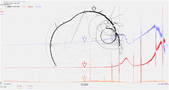
This is the antenna on its own, no matching components yet, I'm measuring using U-FL:

This is after adding the first C from the load, named "A":

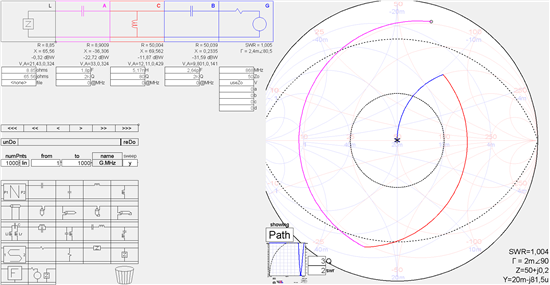
That is nice, it follow what I want to do.

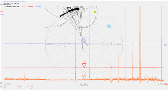
However, by adding the L, named "C" it does not seem to behave as expected. Blue square is where I want to go, as in the first picture. Green is where I really go when placing a L=4nH. Thus, to go to Blue square I decided to increment L to 5nH. However, I finish here at marker "1".

So, my question is:

  1. Do you recognize which may be my problem? It is not even following Smith Chart rules! My GND plane is quite small because of layout demands.
  2. I'm placing 0402 inductances as in the Antenna DK. However, I've seen many places and Application Notes which use 0603. Do you think this can be my problem?

Ok, have a nice day. I hope someone can illustrate me :)

  • Kazola - 

    have you seen this app note? 

    http://www.ti.com/lit/an/swra227e/swra227e.pdf 

    looks like they start out with R +jXL of 29.6 +j11.20 (see page 7)

    you seem to be starting with different value

    I just duplicated their results with my Smith Chart tool - maybe give that approach a try?

  • Our ref designs uses 0402, this is normally better than 0603 due to smaller parasitics. I haven't been able to look into this in detail but check if you didn't do the same mistanke I did, swap antenna and load in the figure. What happens if you swap A and B?
  • Hi Josh!

    Yep, sure I have seen that AN. The initial value depends on your antenna, your GND plane, your layout.... TI design in that AN is much more feasible, since it is more centered in the Smith Chart from the beginning :( I'm afraid my design is too far at the outer edge!

    TER,

    well, I've checked, the antenna is the load, isn't it? In my first attempts I was doing this mistake but not anymore. I have to match my 50 ohm to what I measure in the antenna feedpoint, ZL = 8.86 + 65.56j. From this feedpoint to the U-FL connector where I attach my VNA there is only 1 cm, so it does not act as a transmission line at 868 MHz, so its effect can be neglected.

    So, are all my assumptions right? Am I doing something wrong? Which can be the cause of my board not following Smith Chart behavior? :)

    Have a nice day and thank you both for your attention!

  • Using a smith chart program I started from your second datapoint, rounded to (5 - j29). If I add a 4 nH shunt I end up fairly close to your green dot and if I use 3 nH instead of 4 nH I end up closer to your marker.


    First try to adjust the value of the first cap so you are on a circle directly to the 50 ohm in the middle. Real components will always give a slightly different trace than ideal due to parasitics. See if adding a shunt L move you in the correct direction. Make sure that the correct component values are used. It looks like your method is correct but that something cause the adding of the second component to go wrong.

  • Thanks TER,

    yes, using software simulations in Smith Chart it really goes to the middle.

    However, my problem is that when soldering the real components, the thing does not behave as expected.

    Is it possible I have a GND plane which is too small?

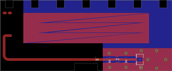
    I attach a picture of my board.

    I will keep trying.

  • What you quite often will experience with a small ground plane is that the impedance is very dependent on the surroundings. If you place the board differently, place something close to the antenna etc do you see the impedane change? Are your measurements repeatable?

  • Hi TER,

    thanks this is unvaluable information. Yes, it really varies. So I should have a good, big ground plane to provide me with more constant behavior, more inmune to changes. Is this assumption right?

    In fact, I'm able to reproduce and do the designs as in your Antenna DK. It is awesome and docs, too. Congrats. However, in our product we do not have the amount of ground plane of the designs in the DK, an we even have some metal surrounding the antenna :(

    I know antennas should be matched in their final placement. How can antennas in the cellphones perform so well in a variety of situations? They are even close to the battery and metal inside the phone! Are they using some isolation material?

    Finally, would you use a PCB trace or a chip antenna in the design in the pictures above?

  • It depends on how you plan to use the product. If your device will have known surroundings a small ground plane is ok since you can match the antenna for this setting. You just have to take care when you do the matching so you actually do the matching with the same conditions as you will have in the application.

    When they match the antennas for cell phones they use a final phone and a fake hand and head to take into account the actual usage. So if you use handsfree I guess you risk de-tuning the antenna since the near field will be different.