This thread has been locked.

If you have a related question, please click the "Ask a related question" button in the top right corner. The newly created question will be automatically linked to this question.

LMX2492 Readback (Using microWire/SPI)

Other Parts Discussed in Thread: LMX2492, CODELOADER, USB2ANY, LMX2581

Hi guys,

My design utilizes an LMX2492 evaluation module to to control an external VCO circuit. The trouble I am having does not involve the VCO or any kind of filtering, but rather the microWire interface. In the datasheet it addresses how to write to the registers. Simply send 16 bits to define the address followed by 8 bits that you would like to load into the register at that address. I have probed the microWire header with a logic analyzer and verified this
(write) protocol. The problem comes when I try to setup readback from PLL to identify and verify what is in each register. The user guide specifies how to do this:

"Note that position 3 is MUXout, which can be used for readback. In order to do this, the MUXout pin needs to be programmed to Readback and also resistor R68 needs to be placed."

I followed these instructions. I populated R68 and using the CodeLoader software I set MUXout_MUX=Output Readback and set MUXout_PIN=Output - PP. Using the CodeLoader software to read from a register, I do not see any activity on the MUXout pin (or any of the pins besides Data, Clock, and LE). After pressing the read button next to a register, it displays it as 0x18. If I press read again, it displays the register as having the value 0x00. If I continue to press it, that value remains.

On another note regarding the readback issues: If I load a value into the register (again using the CodeLoader software) and then attempt to read it back, it never shows me the value I typed in. Typically it will either show 0x00 or 0x18.

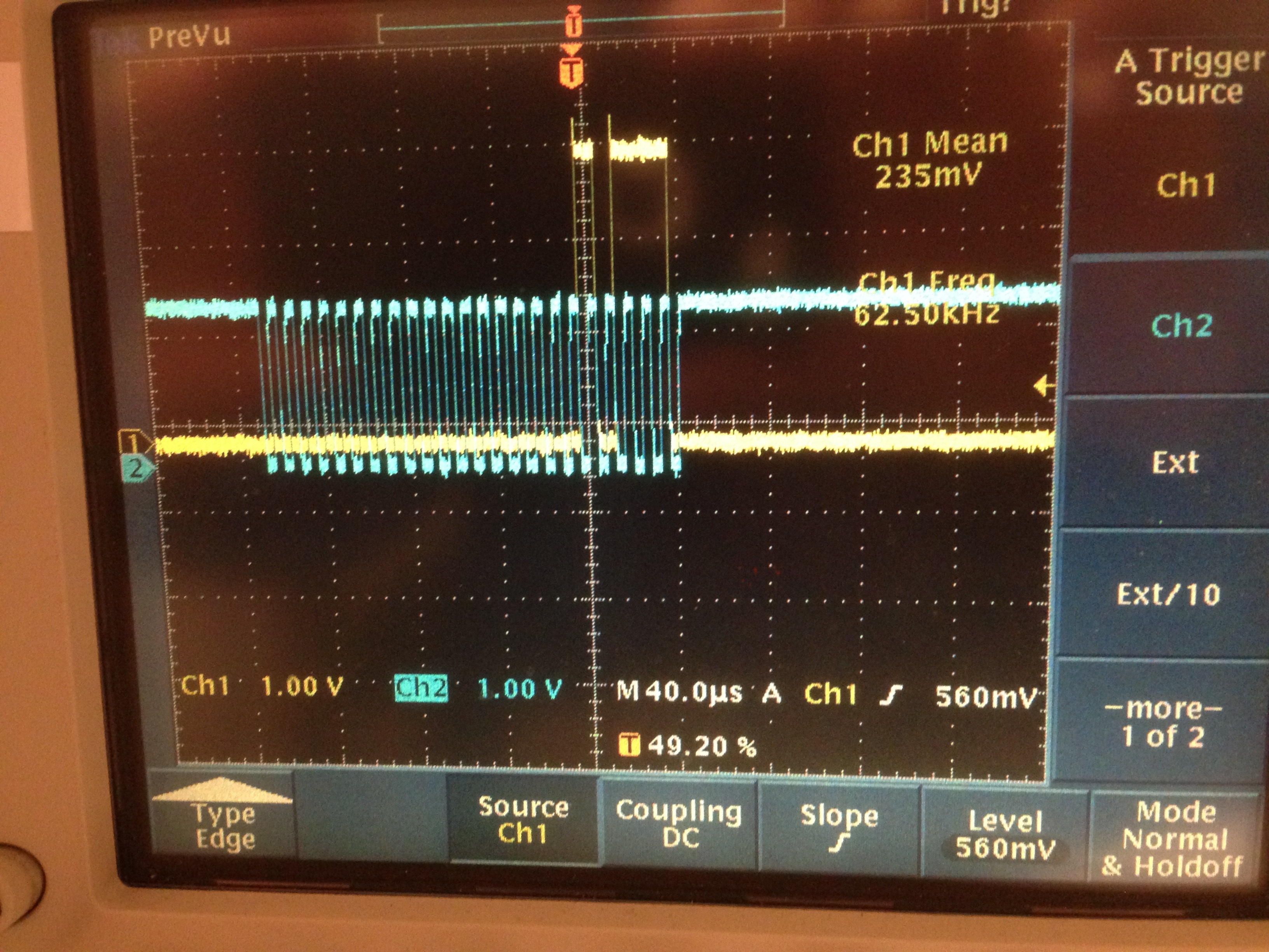
What values must be sent to read a register? When I probe the Data pin while pressing the read button for a register (using CodeLoader) I see the following:

After a read command (for register 0x15), it seems to send one clock (1 data bit = 0) followed by a delay. After the delay, the is a transmission of 24 bits.

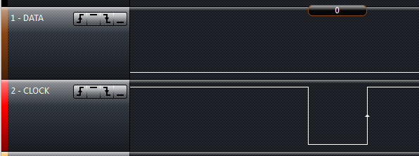
This is close up of the initial clock signal.

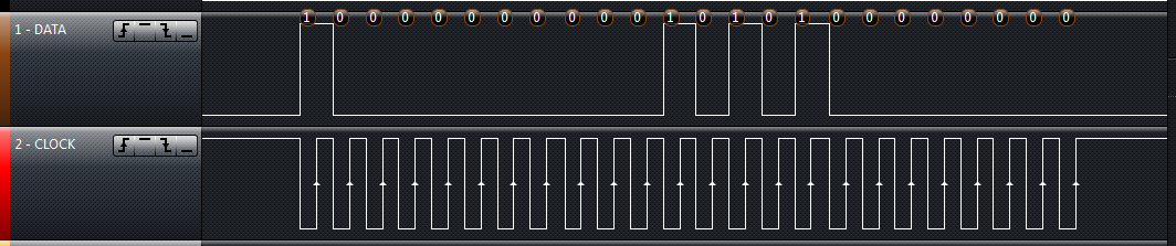
This is a close up of the 24 bit transmission following the delay. It is equal to 0x801500. Am I correct in assuming that the (read) protocol is to send a single low bit, then to wait for a certain period of time, then to send 24 bits with the leading bit being high and the following bits being used to specify the register that we would like to read from? Should the final byte always be 0x00? Should the value of the register be seen on the MUXout pin following this command?


My questions are as follows:

  1. Does it sound like I have things configured properly to read the registers?
  2. Should I be seeing activity on the MUXout pin when the PLL is reading back?
  3. After the PLL is setup to readback, how does the microWire device request the values of certain registers?

Thanks for your help! Please let me know if I need to elaborate on any details about the problem.

Regards, Jack

  • Jack,

    For the LMX2492, the address and data are different than other parts we have done and the readback through the CodeLoader and USB2ANY do not work.  When you push "Read", bits are sent, but then it zeros out the address, this is a software issue.

    As for the no activity, I have got this to work, but if the information is all 0's in the registers, you will get no activity.  WHen you press the "read" button, it zeros out the register, so the second time, you doget zeros.

    In general, using Readback through CodeLoader for the LMX2492 will likely lead to frustration until we fix the CodeLoader.  If you want to verify you are writing, I suggest to write a command that makes the chip react in a known way, such as toggle the MUXout pin from low to high or powerdown the device on and off.  

    In terms of the description, the LMX2492 datasheet has less information, but the LMX2581 has a more complete description of hte timing for readback http://www.ti.com/lit/ds/symlink/lmx2581.pdf.  I know this is the wrong datasheet and readback is not the as the address comes first, not last and there is a R/W bt.  Nevertheless, it at least shows the timing.  


    In response to your questions:

    1.   Yes, it seems like things are setu up properly, but don't trust the USB2ANY or CodeLoader for reading back and also make sure that you are reading back a non-zero register.

    2.   Yes, you should see something.  See what I got below from the LMX2492

    3.   CodeLoader does this automatically with the read button.

  • Is there a more complete technical description of data readback that supplied by the datasheet?

    I am doing readback on MUXout, in my case the PLL is being driven by a microcontroller thus I am not using code loader. I know my write access to the device is working as I can toggle the Muxout pin by setting it output high/low.

    When i set register 0x27 to 0x39, selects readback on muxout and sets this pin as an output, this is an assumption as the datasheet doesn't give any information on what really needs to be done here.

    Then I clock 24 bits with r/w bit set and address set, I see no activity on the muxout line, I have tried a few different registers so it's not the case that zero's are being clocked out in every case.

    Can you confirm if 0x27 set to 0x39 is correct for readback. Do I need to set the MSB to 1 for readback? Should I see bits being clocked out on muxout from clk pulse 16 to 24, after the address has been sent?

    Thanks

    Tony

  • Nevermind, I have this working now!
  • I'm running into this exact problem.  I'm not using Code Loader.  Was able to program the registers successfully, but completely unable to get the read back working.  Would love to know what the issue was.

    Already tried sending: 0x0 0x27 0x3A (MUX, read back, push-pull output).

    I've tried pulling the LE line high after sending the address bytes.  I've also tried sending 0x80 0x27 0x3A as the serial timing diagram on the LMX2492 data sheet seems to indicate the MSB byte of the register address might control Read/Write functionality.