This thread has been locked.

If you have a related question, please click the "Ask a related question" button in the top right corner. The newly created question will be automatically linked to this question.

single-ended to differential converter for IQ inputs of TRF370417

Other Parts Discussed in Thread: TRF370417, THS4509, THS4509EVM, TRF370417EVM, DAC38J84, DAC3283

Hello,

My IQ outputs are single-ended, 200MHz sinewave, 1Vpp, 50 ohm, and DC coupled.  I am looking for a single ended to differential converter, so that I could feed the IQ signals to the inputs of TRF370417.

Do you have any recommendation?

Thanks,

Mark

  • Mark:

    There are a few options.  You could utilize a transformer; however, you will still need to inject the proper common mode voltage for the modulator.  An easier approach is to use the THS4509 as a buffer.  This device can convert from SE to Differential and can set the proper common mode voltage for the modulator.

    --RJH

  • Hi RJH,

    Thank you for the reply.

    If I use the THS4509EVM, do I need to disconnect R7 and R8 (see Figure 94 of slos454h.pdf)?

    Best regards,

    Mark

  • Hi RJH,

    Also:
    Why the typical BW for baseband input is 1GHz? If the IQ signal input is 200 MHz, would it work with this device: TRF370417? And does TI have any single ended input IQ mixers in the similar frequency ranges?

    Best regards,
    Mark
  • Hi RJH,

    Also:
    Why the typical BW for baseband input is 1GHz? If the IQ signal input is 200 MHz, would it work with this device: TRF370417? And does TI have any single ended input IQ mixers in the similar frequency ranges?

    Best regards,
    Mark
  • Mark:

    The typical BB BW spec references the maximum signal bandwidth the input baseband circuitry can support. In this case it is 1 GHz. Anything lower is perfectly fine so you are good at 200 MHz.

    TI does not have any SE modulators. It is possible to drive the TRF370417 SE, but you will need to be aware of a couple of things.

    1. BB Vcm must be maintained on all BB input pins, even the ones not used.
    2. Operating SE will automatically incur 6 dB of loss. This will have impact to gain, IP3, and noise performance of the device
    3. Carrier Feed-through may get a bit worse since the DC levels/loading on the BB ports are not identical

    --RJH
  • Hi RJH,

    If we drive the TRF370417 SE, should we ground the Ns with resistors? If so, what value would you recommend?

    Also, could we drive the LO SE?

    Best regards,
    Mark
  • Mark:

    No, leave the unused terminals open circuit/high impedance. You will need to supply Vcm to those pins. That can be done with a pull-up/pull-down resistor such that the voltage divider yields 1.7V at the pin. Keep the resistor values high to maintain high impedance. These pins will pull very little current.

    The LO can be driven SE. AC couple the unused port and terminate with 50 ohms.

    --RJH
  • Hi RJH,

    Thank you for the reply.

    If I use the THS4509EVM with TRF370417EVM, do I need to disconnect R7 and R8 (see Figure 94 on page 32 of slos454h.pdf)?

    Best regards,

    Mark
  • Mark:

    Correct. For the output connection you will not need any series or shunt resistors (or obviously transformer). The outputs can be directly connected to the modulator BB inputs. --RJH
  • Hi RJH,

    If the power supply is 5V or 2.5V, what would the voltage divider values you could recommend for the unused pins of TRF370417?

    Thanks.

    Best regards,
    Mark
  • Mark:

    I am not following. If you are using the THS4509 as a SE-to-Differential converter then there will be no unused (BB) pins on the TRF3704 device. I think that you are asking the modifications on the THS4509 TI EVM itself. If so, I would remove the series resistor R7, R8 and place 0 ohm jumpers at R9, R10. Then you can use the SMA connectors at J7, J8 to connect up to the differential BB inputs of the TRF3704. You will need one set-up for I-channel and one for Q-channel.

    --RJH
  • Hi RJH,

    Sorry about the confusion!  When I asked about the value of the divider, the solution is without THS4509.

    Best regards,

    Mark

  • Mark:

    The goal is to get 1.7V on the unused pins so a simple voltage divider will do the trick:

    Vcm = Vcc * (R2/(R1+R2)).

    For example, with a Vcc = 5V and R2 arbitrarily set to 2.2kohm, then R1 is calculated to be 4.3 kohm.  There are several combinations that work.  Keeping the resistor values in the kohm range minimizes current and keeps impedances high.

    --RJH 

  • RJH,

    Thank you for the reply.

    My IQ SE signals is 1 Vpp, 50ohm.  Could it be connected directly to the R2 in your above example (VR2 =1.7 V = Vcm), or should it be reduced to mV range?

    Best regards,

    Mark

  • Mark:

    The voltage divider discussed above applies to the unused pin to set the common mode voltage. The other pin is connected to your source (which should be at 1.7Vcm). A 1 Vpp signal is OK as the input to the BB pin.

    If your source cannot provide the 1.7V Vcm then a circuitry is required to do so. The circuitry is dependent on the source. If it is from a DAC then the load requirements of the DAC must be taken into account. If it is from an amp, then the impedance of the amp must be taken into account. The THS4509 op-amp is a nice buffer because you can set the output common mode voltage and then connect it directly to the BB inputs.

    --RJH
  • Hi RJH,

    I am using the SE with TRF370417EVM: I and Q is 200 MHz, 1.84dBm, then passing them through a Bias-Tee with 1.7Vdc; LO is 1.8G, 8 dBm again passing through a Bias-Tee with 1.7Vdc; Power supply: 5V.

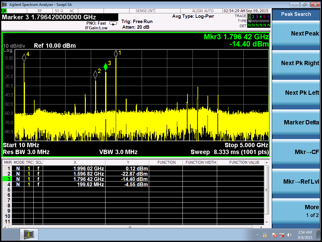
    Measuring at the output of RF, the carrier feedthrough is 22 dBc (-14 dBm), the Lower sideband is -22 dBm, and the upon sideband is 0.12 dBm (see the attached file).

    The test results are far from the numbers in the datasheet (see page 4 of trf370417.pdf: carrire feedthrough: -40 dBm, sideband suppresson: -50dBc).  

    Could you please let us know the reasons for such differences?  Thanks.

  • Mark: Please see below.  --RJH

    I am using the SE with TRF370417EVM: I and Q is 200 MHz, 1.84dBm, then passing them through a Bias-Tee with 1.7Vdc;

    RJH>> This is OK.  I assume that the unused pins are also going through the bias-tee to supply the 1.7Vcm.

    LO is 1.8G, 8 dBm again passing through a Bias-Tee with 1.7Vdc; Power supply: 5V.

    RJH>> The LO signal does not need a common mode voltage.  You can AC couple to one of the ports.  Terminate unused port through blocking cap to 50 ohms.

    Measuring at the output of RF, the carrier feedthrough is 22 dBc (-14 dBm), the Lower sideband is -22 dBm, and the upon sideband is 0.12 dBm (see the attached file).

    RJH>> Carrier feed-through is caused by DC offset imbalance between all of the ports.  With your set-up it is difficult to precisely match all of the voltages.  Very small imbalances translate to the degradation that you are seeing.  If you have fine independent control of each voltage on the bias-tee you can tune the voltages and actually null the carrier.

    The sideband suppression is caused by amplitude and phase imbalance between I/Q paths.  Again, for your set-up with a bias-tee and cabling it is difficult to keep the amplitude and phase perfectly balanced.  Amplitude imbalance on the order of a couple of tenths of dBs and phase imbalance of a couple of degrees will cause the degradation you are seeing.  Unfortunately, there is not an easy way to tune out the imbalances in your system.  If you have independent control of the I/Q amplitude, you can adjust the input power slightly on one branch to optimize the amplitude imbalance.  For the phase, you can try to insert a connector saver adapter in one of the paths to give a little extra length to tune the phase response.

    If maintaining good CF and SBS performance is critical, the DAC like a DAC3283 or DAC38J84 is the path to go since those devices can keep DC offset and amplitude/phase balance well and they have adjustment features to null the carrier and unwanted sideband.

  • Hi RJH,

    Thank you for the reply!

    We have tried the THS4509EVM with the TRF370417EVM.  The setup is the following:

    1. single ended I & Q: 200MHz, - 4dBm to THS4509EVM to J2 of THS4509EVM,
    2. removed R7, R8 of THS4509EVM
    3. shorted R9, R10 of THS4509EVM
    4. using 6" SMA cables to connect J8, J7 to the TRF370417 J4, J3 for I, J6, J5 for Q
    5. apply +5V to Vs+, 0V to Vs-, GND, +1.7V to TP2
    6. connect 50 ohm termination to J2 of TRF370417EVM
    7. connect 1.8GHz, 10 dBm to J1 of TRF370417EVM
    8. apply 5V to TP2, TP4 of TRF370417EVM

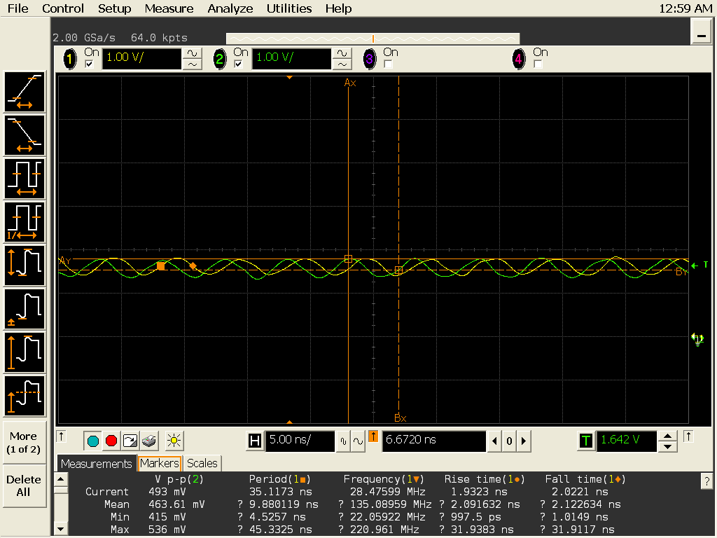
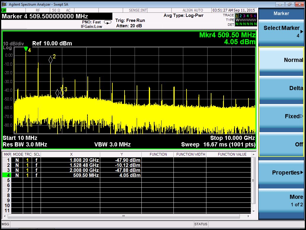
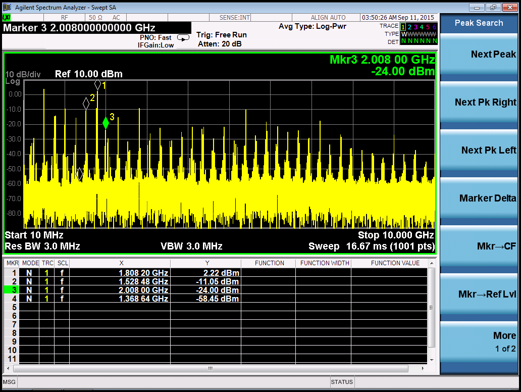
    What we have found is that there is a lot of spur, as soon as the Vcm =1.7V turns on.  Any comments on that?

  • Mark:

    This looks like harmonics; however, there is something strange.  The LO is ~ 2GHz (1.8GHz).  The BB is 200 MHz.  There are some high spurs at ~500 MHz, ~1 GHz, and ~1.5 GHz that I do not understand.  Further, I do not understand the difference between the two plots.  The lower one does look fairly bad.

    The THS4509 may be going unstable.  The THS4509 does not like to drive low impedance.  The 6 inch 50 ohms cable may be enough to cause an issue.  Try to get even shorter cables if possible or use a combination of right angle adapters to eliminate the cables altogether.  I know this is tricky when connecting two EVMs together.  Alternatively, connect the two devices with just equal length, short wires.  This will increase the impedance.

    Make sure that you are not over-driving the THS4509.  That may be causing some strange distortion that you are seeing.  Back very far off and slowly come back up to desired output signal level.  Also, try to back off the LO drive level to 0 dBm.  Once stable, you can experiment with increasing LO drive to get linearity and output noise improvement.

    --RJH

  • Hi RJH,

    Thank you for the reply.

    Sorry about the confusion regarding the attachments.  I thought the name of the file would be attached as well.

    The first one was all powers were on, but the LO and IQ were off.  The second one was all powers on and LO and IQ were on.

    Best regards,

    Mark

  • Hi RJH,

    Could we use connect the unused pins directly to 1.7 V through a high value resistor, such as 2.2 Kohm, without using a voltage divider, if we are using single ended inputs for TRF370417?

    Best regards,
    Mark Liang
  • Yes, that will likely work. --RJH
  • Hi RJ,

    We have the following questions regarding TRF370417EVM:

    1. In 1.4 and 1.4.1.4 of the EVM user's guide: SLWU062, it mentions that 0.85V is used for common mode I/Q offset.  Yet the common mode voltage is 1.7V for TRF370417 from the datasheet.  So if we apply I, I bar, Q, Q bar to the p/n of the IQ of TRF370417, what offset we should use?
    2. What input impedance of the input ports, i.e. I, I bar, Q, Q bar, should be?  We have found that the input impedance of the two cards, which we ordered, have different values from 0.7 Mohm to 0 ohm.
    3. Could we have conference call to discuss this further?

    Best regards,

    Mark Liang