This thread has been locked.

If you have a related question, please click the "Ask a related question" button in the top right corner. The newly created question will be automatically linked to this question.

LDC1614 Reference Clock Input Load

Other Parts Discussed in Thread: LDC1614, CD74AC244, CDC203

Hello,


I´ve got a question about LDC1614.

I want to use a oscillator to run multiple LDC1614, so I thought about using a 3.3 V HCMOS oscillator. For this I need a buffer because of output load of each chip. How much is the output load of each LDC1614 chip?

Thanks for your help!

Best Regards

Tim

  • Hi Tim.

    I will need to get back to you on this. How many LDC161x devices were you planning on using? You may consider using a buffer, such as a CD74AC244.

    Regards,

    ChrisO
  • Hi ChrisO,

    thanks for the quick reply. I want to use about 30 LDC1614 chips. For this I thought about using clock buffer CDC203 from TI, because I can load 5 chips on every output.

    Regards,
    Tim
  • Hello Tim.

    Would you be able to use the IBIS model provided for the LDC1614 (www.ti.com/.../snim004)? The capacitance of the CLKIN pin is about 1pf, but that does not include any other parasitics. You will need to be careful with the design you propose - it can be quite easy to have ringing and other transmission line effects if you need to distribute the clock lines more than a few cm. When you route the traces, you may wish to use a series termination resistor where you fanout each of the CDC203 outputs.

    Regards,

    ChrisO

  • Hi ChrisO,

    thanks for the link to IBIS model of LDC1614. There I can see, that input capacitance of LDC1614 CLKIN pin is about 0.2 pF and inductivity about 1 nH. If I want to attach 4 LDC1614 to one buffer output. Can I sum up the load of every chip for impedance match?

    Moreover would it be better to use parallel termination instead of series termination? With series termination and impedance matched trace thickness there will be even a voltage divider. Atfer reflection there will be full amplitude of signal. But before there is only a half of it. With CMOS the threshold could interpret any parasitic effect as wrong clock signal.

    I tought about using AC (resistor and capacitor) or parallel (resistor) termination. Is this a better solution?

    Best Regards
    Tim

  • Hi Tim.

    Yes, a parallel termination provides many nice characteristics, however you will need a very high current drive - if you are fanning out one output to 5 LDC1614s, each with a 50 parallel termination, then each output will see 10ohms to ground.

    Regards,

    ChrisO

  • Hi ChrisO,

    You´re right. With 3.3 V and 50 Ohm parallel termination I need a high current drive of the buffer. Is there any buffer from TI with fanout of more than 30 mA? Then I could think about using only termination at the end of the 4 LDC1614 chips. Otherwise I will think about series termination. But then I need to use several outputs - every LDC1614 chip needs a single series termination. This would be very complicated because I want to use 30 chips.

    Best Regards
    Tim
  • Hi Tim.

    I think that a series termination structure will suit your needs better, as you won't have significant power being burned in the termination resistors. However, the routing needs to be carefully designed, otherwise you will have lots of transmission line effects. Be careful with long traces (I would pay attention to any traces longer than 5inches, especially if they were Y splits), and make sure that all traces have continuous ground planes underneath.

    On another note - how will you communicate with all 30 LDC161x devices? Do you have 15 I2C peripherals, or are you using an I2C multiplexer, or are you putting several devices into shutdown?

    Regards,
    ChrisO
  • Hi ChrisO,

    thanks for your reply.

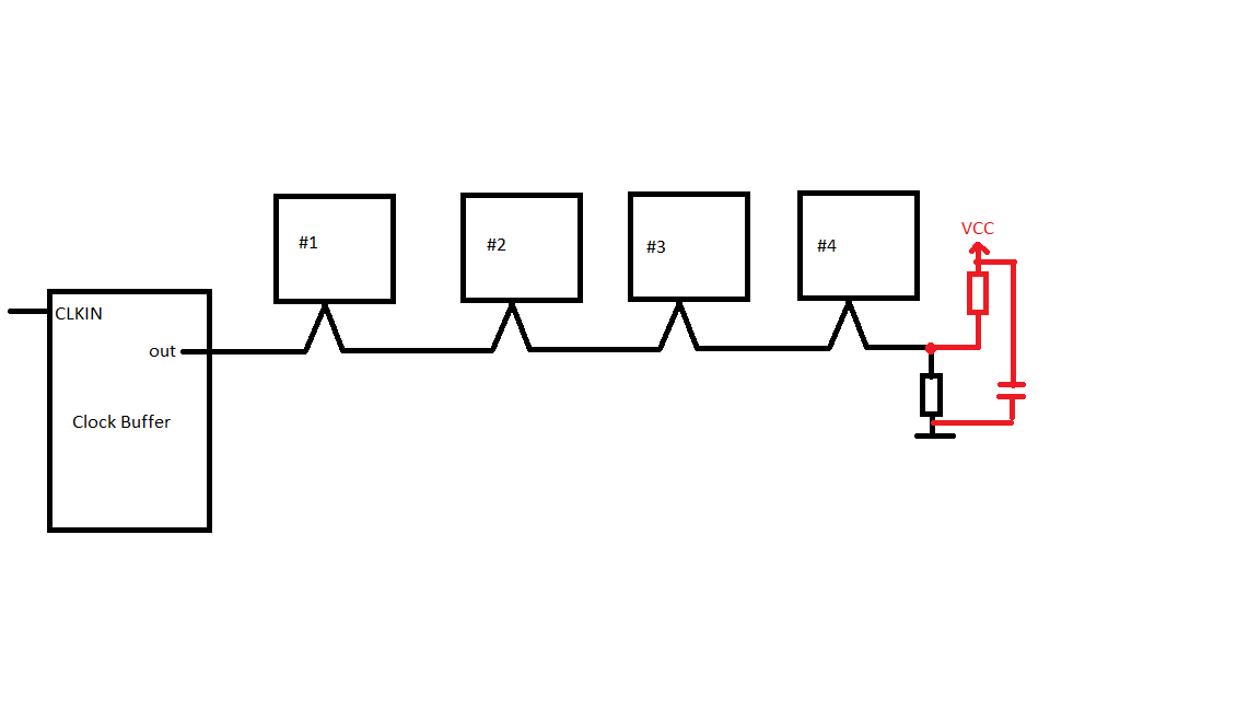
    I won´t route traces longer than 5 inches because I use a clock buffer for clock distribution. I will think about series termination. What do you think about Thevenin termination using clock signal for 4 LDC1614 as you can see in the following figure?

    I will communicate to all LDC1614 devices by putting unnecessary devices into shutdown mode, because I don´t want to have interferences due to other working LDC1614´s.

    Best Regards

    Tim

  • Hi Tim,

    it is possible to use series termination for several receivers from one buffer output by adding one series termination resistor for each transmission line close to the source. Would this approach work for you?

  • Hi Ben,

    Yes, thats a good idea. But I think there could be a problem because of different length of traces. I wanted to have only one Transmission line for every buffer output. Is there maybe anything else working with configuration seen in figure above?

    Thanks a lot for your reply!

    Best Regards
    Tim