This thread has been locked.

If you have a related question, please click the "Ask a related question" button in the top right corner. The newly created question will be automatically linked to this question.

TMP007 Layout in Flexible PCB

Other Parts Discussed in Thread: TMP007

Hi TI,

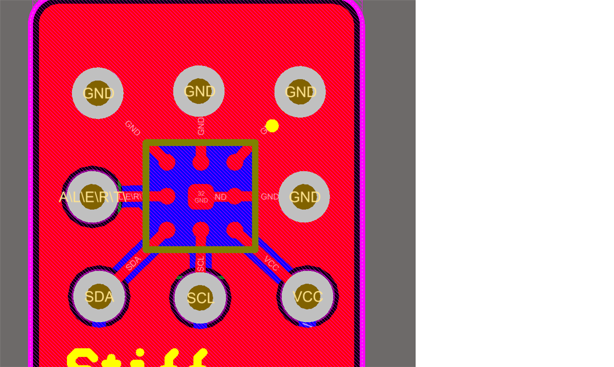
I am designing a product and have chosen TMP007 for our temperature sensing needs. Our design in a double-sided Flexible PCB with 0.2mm thickness and Polyimide Stiffeners. I have followed the layout reccomendations provided by your white papers, and i am also attaching a picture of my layout for your reference. 

The problem is that we have a 30% failure rate on the TMP007 sensor (3 out of 10) , with pick and place machinery. Is the idea of mounting tmp007 on a flexible PCB too ambitious, or there are ways i could optimize my layout for better performance? 

Please note that tmp007 is on the first side that is reflowed, next is the opposite side. 

Thanks,

Timos
  • TI support team will contact you shortly.
  • Hi Tim,

    How do you define defective?

    This device has a cavity with laminate covering in the center of the device. It's possible to damage this covering during assembly either due to improper handling or solder/flux contaminants beneath the device. Our customers commonly struggle with this, so I don't think your issue is unique to flex.

    When the device is damaged in this way, it will have little to no voltage response (in the Sensor Voltage Register 0) to infrared radiation. You should be able to hold a hot object directly in front of the device and see hundreds of microvolts in this register.

    Thanks,
    Ren
  • Thanks a lot for your answer Ren. Sorry, defective was not the right word, we just couldn't communicate with the sensor at all. 

    Seems that i have found the problem. I had not expanded the Top Solder mask a bit more than the actual pads, so the pads were barely out of the Solder Mask due to Flexible PCB manufacturing imperfection. Whoever has similar problems with TMP007/006, look for DSBGA NSMD pads folks. 

    I have one more question, regarding the standard mounting method. Should the 15x15 mil copper area under the sensor  be filled with solder mask or should be left exposed for better thermal equiibrium? 

    Thanks!

  • We built our EVM with the solder mask removed. We use gold (ENIG) finish plating. If you are using a cheaper finish plating, you might be better off covering the copper with mask. We have also built boards this way, and have had success with them.

    You can also read this similar post:
    e2e.ti.com/.../2255878

    Ren