This thread has been locked.

If you have a related question, please click the "Ask a related question" button in the top right corner. The newly created question will be automatically linked to this question.

DRV5053: Variation in output from changing Vin

Part Number: DRV5053

While using a DRV5053OA device, we have noticed that the output voltage is varying when the only change made is to Vin. Our application is battery powered, so some reduction in voltage must be expected. The voltage has not been dropped below 2.8 V in our testing, and yet we are seeing changes in the output voltage. There appears to be no mention of this within the data sheet, and so we are wondering if this is expected, if there are any numbers / formulae we can apply to allow our application to properly track the output with respect to input voltage. Or - is this a fault with the particular piece we have on our test board. Currently we are seeing a variance of approximately 30 mV on the output signal for a 100 mV variance in input voltage.

  • Hello Berin Casey74,

    Thank you for your interest in the DRV5053. Power supply sensitivity of analog circuits (including the DRV5053) invariably degrades at high frequencies with open-loop gain. So you may observe output fluctuations if there are high-frequency changes in the supply voltage.You are also likely to see output fluctuations if you have a high-frequency load on the device that changes with supply voltage.

    What kind of stimulus are you applying to Vin when you observe the unexpected output response? Btw, I am assuming that by "Vin" you are referring to pin 1 of the DRV5053. It would be helpful if you could post o-scope shots of the Vin waveform as well as the part's output response, along with a schematic of your circuit and a brief description of your test conditions.

    Best Regards,

    Harsha

  • Harsha,

    Thanks for getting back on this.

    We are applying NO stimulus to the supply voltage (Vin). We are simulating the gradual decline of battery voltage over time, so have set the voltage at, for example, 3.5 V, and allowed time to settle (> 1 s) before taking readings. We then change the voltage to, 3.4, 3.3, &ct then leave a settle time again before taking readings.

    I cannot upload schematics, as they are commercially sensitive. Perhaps you can supply me with an email address that I can send them to, as a public forum is not an appropriate place for professional technical support.
  • Thanks for clarifying. The transfer function of the DRV5053 is of the form VOUT = B x sensitivity + VQ. Based on the plots in section 6.8 of the datasheet, sensitivity and VQ have minimal dependence on supply voltage. The question now is what about B? What kind of magnetic source are you using? Does it stay constant (or ideally zero) for the duration of your test? Also, do have any boards that are behaving correctly, and if so have you tried swapping devices to see if the faulty behavior tracks?

    I have sent you a request to connect over private messaging if you'd like to share relevant debug information more securely.

    Best Regards,
    Harsha
  • Again, thanks for your response.

    In our application, we have a permanent magnet as a source. The actual magnet changes, but for the purposes of the tests we only use one at a time. The magnet is held in place on a test jig, where we can change the position of it. During our testing we have used a magnetic source held in a fixed position, and also have had all magnetic sources removed from the test jig. Both scenarios have given us this problem with the supply voltage variations. We do not have any boards behaving in a different manner than outlined.
    We have more testing planned, and I hope to not have to provide debug information - though obviously if our further testing is unsuccessful then I shall share via PM.
  • Hello,

    One debug strategy would be to start with the simplest test conditions and check for correlation with the datasheet. If the faulty behavior persists then you may have received a bad batch of parts or perhaps there is something wrong with the measurement path. Otherwise, this may be an application issue. To isolate root cause, we can then start tweaking the input variables (i.e. supply, load, input) one at a time to match the application conditions (or try various permutations and combinations) until the faulty behavior occurs. 

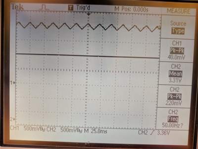
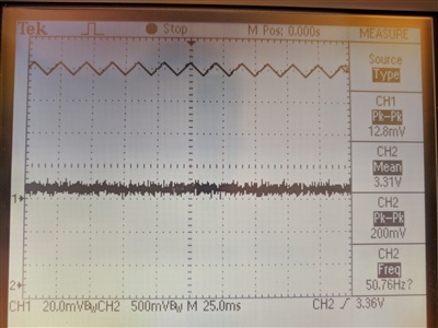
    For your reference, I measured the response of a random DRV5053 sample to a low-frequency power supply ripple waveform with no supply bypass cap, no input field and no load applied. VCC and VOUT were measured with respect to the chip GND pin. My observations are captured in the pictures below.

    CH2 depicts the VCC signal consisting of a 200mVp-p ramp @ 50-Hz fundamental, superimposed on a DC component of 3.3V driven by a clean DC power supply. With no field applied (B=0) the DRV5053 output sampled on CH1 has a DC value of 1V as expected. 

    Zooming in on the AC component of the output down to 20mV/division which is below the level of variation you are observing, the output is pretty much flat. This behavior correlates with the datasheet.

    Best Regards,

    Harsha