This thread has been locked.

If you have a related question, please click the "Ask a related question" button in the top right corner. The newly created question will be automatically linked to this question.

TS5A23166: Device Power Off characteristics

Part Number: TS5A23166
Other Parts Discussed in Thread: SN74CBT3306

Switch Gurus:

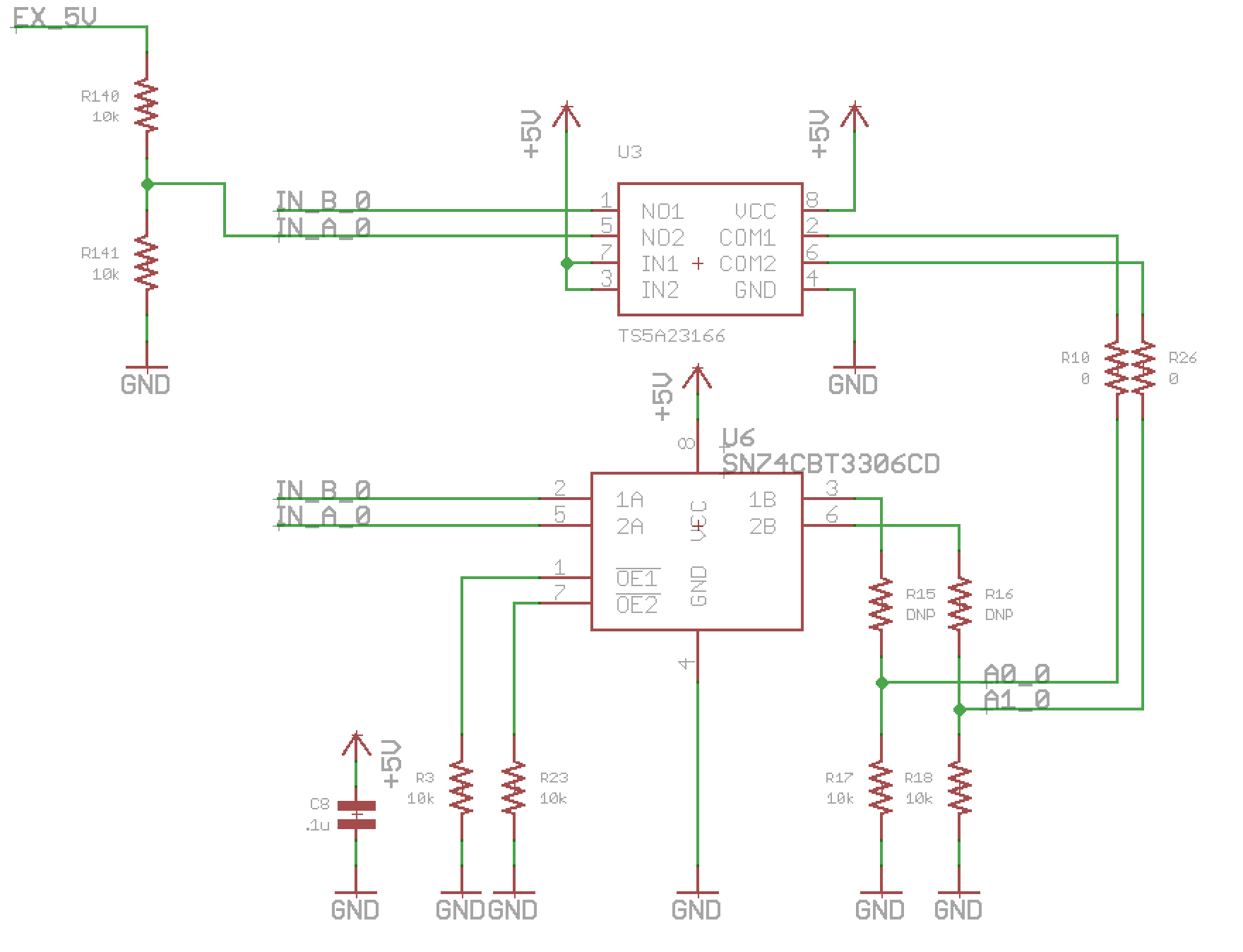
I designed in this device at the recommendation of Dakotah:

https://e2e.ti.com/support/switches_multiplexers/f/388/t/618079

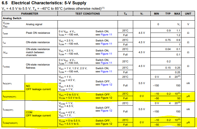
However my client is seeing signals at the NO terminals sink current when the device is unpowered.  I was told this device had IOFF protection.  Is this not the case?

Best,

Trey

  • Hi Trey,

    I just verified in the datasheet that the TS5A23166 does indeed have IOFF protection. This is specified with the device supply pin VCC =0V. I have included a snapshot of the datasheet showing the spec for the NO and COM pins.

    My first question would be at what temperature is the device operating at? As shown in the datasheet the max spec at full temperature range is ±50uA. If this is outside the limit the client is expecting it could be causing undesired signals.

    Can you provide some more information on what signals your client is seeing at the NO pin?

  • Dakotah,

    What I'm seeing is really strange.  I have the device hooked up as follows:

    I've removed the SN74CBT3306 to isolate the issue.  The +5V net has it power switched while EX_5V is always powered.  Under steady state power off conditions, IN_A_0 sits at 2.5V as expected.  When powered on, the voltage drops a bit due to the extra 10k which is now in parallel.

    Now for the weird part... When power is removed from +5V I see IN_A_0 drop to ~1.2V and sit there for roughly 10 seconds before popping back up to 2.5V.  Seems to me like something is latching in this device that shouldn't be.

    Just to prove out my test setup I have another instance of this circuit with the TS5A32166 removed.  This circuit behaves as expected.  I've also verified markings on the devices to confirm the distributor did not make an error.

    Any ideas?

    Thanks,
    Trey

  • Hi Trey,

    Thanks for providing more info on what you are encountering.

    This seems to be related to the Charge Injection (Qj) spec of analog switches rather than that of the Ioff protection. However, it has manifested in such a way that it was encountered when you were utilizing Ioff protection.

    The charge injection is a level change in voltage caused by the stray capacitance of the NMOS and PMOS FETs that create the switch. Because the geometries of FETs, these capacitance are not matched and lead to a redistribution of charge when the switch is toggled. When the Ioff protection is utilized the charge will need to follow the rules of Q=C*V.

    To test this out try placing a load capacitor on your board to minimize the charge injection impact. Because of Q = C*V, a larger load capacitor will lead to a smaller voltage glitch, the trade-off is in the reduction of system level bandwidth.

    Here is a really good precision lab video that talks about Qinj. spec (as well as leakage current).

  • Dakotah,

    Do I need to be loading the NO or COM terminals of this device? I forgot to mention earlier that we already have a 10u cap on the NO terminal net.

    Best,
    Trey
  • If there is already a 10uF capacitor on the NO terminal this should be sufficient to handle change in voltage due to charge injection of the device.

    Can you verify the following test cases:

    1) This event has been observed on multiple units, preferably a new board if possible? (can help ensure device was not damaged from some previous event).

    2) Try changing the capacitor value to see if the voltage change behaves differently with varying values.

    I will see if this can be replicated on a device in the lab. If not, I may contact you via personal message to see if you can send one of your units for further investigation.

  • Hi Trey,

    Quick update, we did not have any units on hand so I went ahead and ordered a few samples for testing. They should arrive by Monday and I can see if what you are experiencing can be replicated.

    I will keep you updated.
  • Dakotah,

    I was doing these tests on a new board on the bench.  This board has several instance of this circuit, but I've only tested  this on a single TS5a... device.  I will try some of the other devices on the board as well as monkeying with the capacitance.  Should have more info this afternoon.

    Thanks for looking into this,

    Trey

  • Tried messing around with the board some more. I'm seeing the clamp state last longer with lower capacitance values :(
  • Trey,

    I was able to test two units in the lab and was not able to fully recreate your issue. I do have a question for you however.

    Is there enough current drive capability on your EX_5V signal? On the two units I tested I am using a DC supply (ideally with infinite current capability) to drive the input signal and the fault protection was working as expected. I then set my current limit to a much lower threshold (few mA) and this would prevent the device from going Hi-Z and the signal would still pass from the NO pin to the COM pin.

    I could not recreate the latch-condition that you mentioned but if your signal does not have enough drive strength it may react different in your system vs. my setup (essentially using a break-out board and some resistors).