This thread has been locked.

If you have a related question, please click the "Ask a related question" button in the top right corner. The newly created question will be automatically linked to this question.

SN74CBTLV3126: Bi-directional Issue

Part Number: SN74CBTLV3126
Other Parts Discussed in Thread: TMUX1511

Dear Team,

Do you have any ideas the root cause it can't bi-directional?

A signals from system CPLD on main board.

B signals from CPU GPIO and OE from CPU CPLD control.

All power sequences are controlled by the system CPLD.

If we connect from B to A in JTAG upgrade, the system will cause shutdown.

Then we exchange the signals of A and B, and the system will be updated normally.

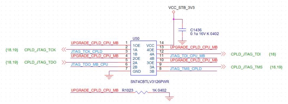
Please help to check the SN74CBTLV3126 schematic.

BR

Kevin

  • Hi Kevin,
    looks strange but for clarification:
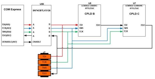
    Your system is an external modul with a CPU and a mainboard with CPLD you want update.
    The CPU enables the switches to the modul and emulates with GPIOs JTAG to update CPLD.
    The CPLD controls the power of the mainboard (if his JTAG is disturbed the mainboard can shutdown).
    The system is working in switch direction B->A but not A->B.

    Reasons for unsymmetrical behaviour:
    - FETs have tolerance, FET A->B is not FET B->A
    - FET B->A has inverter with propagation delay

    Is this the behaviour from beginning? How can you exchange the sides? The switch is part of the mainboard or modul?
    Can you measure a glitch on a CPLD-line when connecting or enabling? (PU/PDs for defined level on CPLD JTAG-lines, capacitor 10nF for CPLD_JTAG_TMS)
    Can you measure a diode-function for a enable/disabled line with multimeter? Can you replace the part?
    I assume defect analog switch part (one FET of a switch is gone or abnormal) probatly of an EFT-event.
    There is no bidirectional signal, why using analog switch?
    BR
    Miko
  • Dear Miko,

    1. What do you mean FETs have tolerance, FET A->B is not FET B->A? Last time I check with your team, they mention it will be like 5ohm resistor. So there will be no problem for bi-directional. For the tolerance do you mean delay time?

    2. What do you mean FET B->A has inverter with propagation delay? I am not sure what do you mean about the inverter part.

    3. We use another board to jump the wire for exchange the side.

    4. They use JTAG to upgrade the code. So will have TDI from A to B and TDO from B to A by a different channel. Currently of the U50 they design with an opposite direction, which will cause the system fail.

    Success:

    Fail:

    Or you have P2P part number can directly replace this one and solve the issue here. Please let me know.

    BR

    Kevin

  • Dear Miko,
    I am not sure what do you mean here:
    Can you measure a glitch on a CPLD-line when connecting or enabling? (PU/PDs for defined level on CPLD JTAG-lines, capacitor 10nF for CPLD_JTAG_TMS)
    Can you measure a diode-function for a enable/disabled line with multimeter? Can you replace the part?
    I assume defect analog switch part (one FET of a switch is gone or abnormal) probatly of an EFT-event.
    BR
    KEvin
  • Dear Team,

    Or you have an easier way to solve this issue please let me know.
    Because the customer is urgent to provide the sample products to the end customer.
    So if you have a suitable suggestion to solve it, they will need to use a small card to jump wire.

    BR
    Kevin
  • Hi Kevin,

    thank you for the pictures, better to understand your system.
    I am not from TI, please correct things if wrong understood, i am not finished.

    1. In datasheet on first page is an simplified schematic of a one analog switch. There are two different FETs (p and n, not symmetrically) between A and B controlled by the Input (OE). FETs have tolerances in threshold voltage, gate capacitance, Rdson etc. . Rdson is like an 5ohm resistor, but look at 6.5 Electrical Characteristics 5<ron<40ohms! Different threshold voltages leads to different switching/delay times. Please note the range at 6.6 Switching Characteristics there are up to 4.2ns-1.9ns=2.1ns difference, this can cause a glitch if you switch simultanously (OE) and a signal at A B.

    Details in http://www.ti.com/lit/pdf/szza030


    2. In datasheet on first page is an simplified schematic. I mean the additional driver between (OE) and the upper FET. It is just a difference.

    This all should be no problem if the part is not damaged and the timings and levels from COM-Express are not critical.

    >Can you measure a glitch on a CPLD-line when connecting or enabling? (PU/PDs for defined level on CPLD JTAG-lines, capacitor
    >10nF for CPLD_JTAG_TMS)
    It is essential to have clear defined signal levels and timing at all cases. Some use TMS as TRESET, thats why a 10nF to gnd can help
    about glitches. In your case TMS is latched by CLK.
    Clear levels can provide additional pullup/pulldown resistors. The CPLD has only weak pull resistors integrated.
    Timing controls the COM Express.
    If you enabling the switch and change the level of signals simultanously you can have a glitch on CLK confusing the CPLD.

    >Can you measure a diode-function for a enable/disabled line with multimeter? Can you replace the part?
    >I assume defect analog switch part (one FET of a switch is gone or abnormal) probatly of an EFT-event.
    Can you replace the part with an other SN74CBTLV3126? I had such effects with ESD-damaged parts.

    I would measure the signals on oscilloscope TDI, TMS, TCK at U5 in both cases (success/fail) to validate levels and timings at
    rising edge of signal UPGRADE_CLD_CPU_MB or just use the jumper card.
    BR
    Miko

  • Kevin,

    I agree with Miko here.  

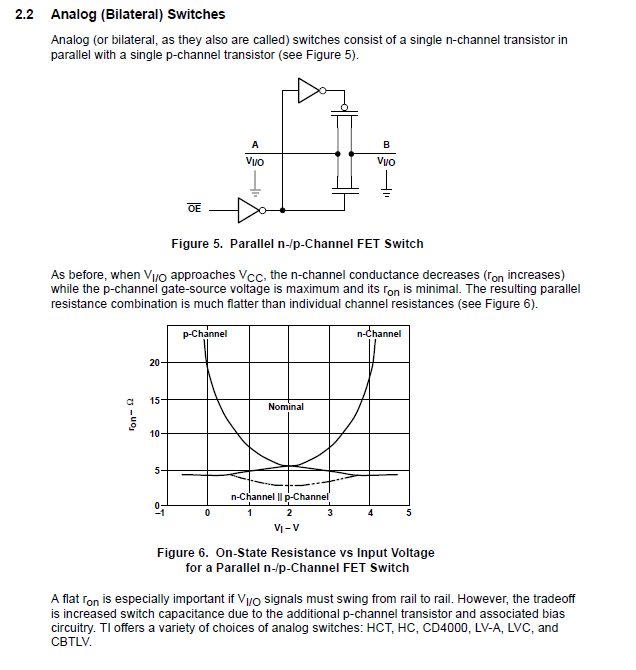
    This part is a bi-directional like all of TI passive switch so there shouldn’t be any issue communicating from A to B or from B to A.  It can be thought of as a series resistor (Ron) and parallel capacitor (Con).  Below are examples of how the switch will behave and showing what Miko was talking about with the two different FETs NFET and PFET.    

    Have you followed the debug steps Miko recommended? 

    1. Did you replace the device and the issue is still present?

    2. If you place the part you removed on a known good board does it duplicate the issue?

    3. Are you able to scope the input and outputs of the of signals to see if there are any differences? 


    The new  TMUX1511 device is a p2p replacement you can try but without knowing the root cause of your issue I can confirm if this will solve your problem.

  • Kevin,

    We haven't heard from you in several days. Do you have additional testing results to share, any questions, or new ideas?

    Thank you,
    Adam
  • Dear Adam,

    The SN74CBTLV3126 still have issue.
    I already provide the sample TMUX1511 to the customer.
    We will have result after 2/11, because next week is Chinese Ney Year holiday.

    BR
    Kevin
  • Dear All,
    The customer change to the TMUX1511 and the issue is solved.
    Can you provide the explanation?
    The end customer want to know the reason.

    BR
    Kevin
  • Kevin,

    I need help from you in identifying a root cause in order to provide an explanation why the TMUX1511 device solves the issue.

    1) Do we know if this was an isolated part defect or part damage with the SN74CBTLV3126?  How many parts fail in your system vs how many are successful?  Does taking a part of a failing board and place it on a passing board cause failure? 

    2) I would measure the signals on oscilloscope TDI, TMS, TCK at U5 in both cases (success/fail) to validate levels and timings at
    rising edge of signal UPGRADE_CLD_CPU_MB or just use the jumper card. 

    I would also repeat this testing with the new TMUX1511 device to compare the signals to observe differences that might show the root cause.

    3) I can tell you some differences between the two devices but I can't tell you if these differences are the reason it solves your problem without knowing what the root cause is. 

    TMUX1511 is a NFET with a charge pump biasing the gate type switch.  This device has lower on-state capacitance resulting in supporting higher bandwidth and will support signal voltages on the I/O pin greater than supply voltage.

    SN74CBTLV3126 is a PFET and NFET transmission gate type switch.  This device supports signal 0 to Vcc.

    Thank you,

    Adam  

  • Kevin,

    Do you have more information on this testing? Do you have a hypothesis of a root cause?

    Thank you,
    Adam
  • Kevin,

    We haven't heard from you in a while so I will assume your issue is resolved and close this thread. If you have additional questions you may post them here to re open them or start a new thread.

    Thank you,
    Adam