This thread has been locked.

If you have a related question, please click the "Ask a related question" button in the top right corner. The newly created question will be automatically linked to this question.

WEBENCH® Tools/SN74TVC16222A: SN74TVC16222A

Part Number: SN74TVC16222A

Tool/software: WEBENCH® Design Tools

Hello TI 

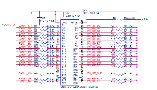
I has some questions about SN74TVC16222A application.

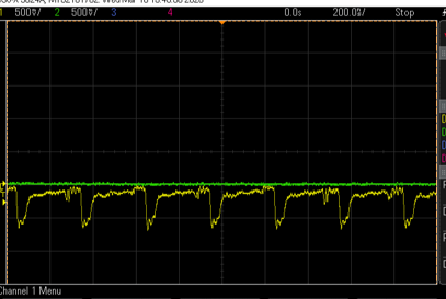
My test environment was level shift between 3V3, 1V8 that I reference the measure circuits. 

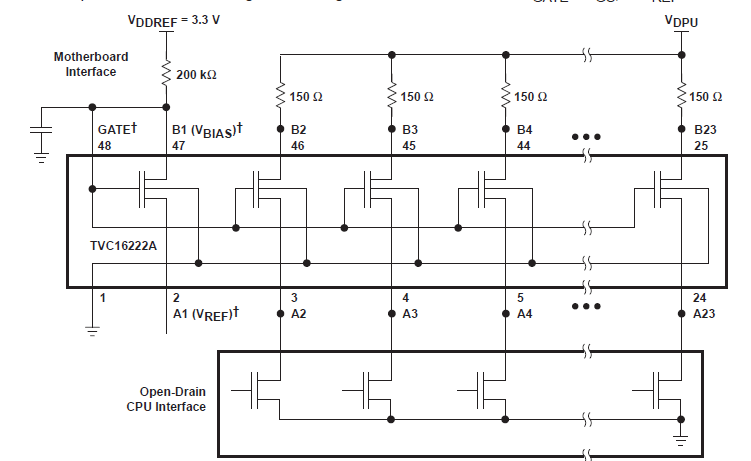
The B side 150 ohm resistance is mean pull high resistance function? why need this resistance? 

This resistance value could be change? for ext : 1K, 2K 

If remove this resistance, Is still work? 

Please reply my question.

Thanks 

Ken

  • Hi Ken,

    This diagram is an example application and you do not have to follow this schematic exactly as shown. 

    The resistors are there likely to limit the pass-transistor current (recommended operating conditions specification is 20 mA typical, 64 mA maximum).

    The resistors may not be necessary for your application. You may design the resistors and other system components as needed to maintain current and voltage within recommended operating conditions.

    Best regards,
    Kate

  • Dear Kate

    Thanks your reply.

    Can you suggest us the circuits to use SN74TVC16222A?

    My application was needed level shift digital signal (data and CLK) form 3V3 to 1V8 (B side to A side). We was already created the daughter board used SN74TVC16222A chip. But CLK signal sometime was unstable and strange.

    left side was OK, right side is NG (CLK high level was disappear)


    This is out level shift circuits. 

    Could you help us to check our design problems ?

    Thanks 

    Ken

  • Hi Ken,

    Thank you for sending the waveforms and schematic.

    You could provide more description of the waveforms?

    • What pins are each of these scope shots measuring?
    • Could you mark the voltage levels for each shot?
    • If this is a digital signal, what is the undershoot in the signal?
    • What is the voltage at VCCO_J1?

    Thanks!
    Kate

  • Hi Kate

    What pins are each of these scope shots measuring?

    => This environment was for FPGA platform. Source side was digital data (D0 ~ D11 and CLK) form digital I/O play card. 

    Could you mark the voltage levels for each shot?

    => The CLK pin level = 6V, (peak to peak level = 7.5V). Data pin level = 4~5V

    If this is a digital signal, what is the undershoot in the signal?

    => The is CLK signal from source side (Digital I/O play card). 


    What is the voltage at VCCO_J1?

    => The VCCO_J1 was form FPGA supply 1.8V power. 

    Thanks

    Ken

    Thanks your reply.

  • Hi Ken,

    Thanks for the additional information.

    To clarify, the scope shots are of the CLK signal path, with a peak-to-peak value of 7.5V? Is this the only channel you are experiencing an issue with?

    The maximum input/output voltage recommended operating condition is 5.5V. Functional operation is not guaranteed beyond recommended operating specifications. This may be why the signal is not passing as expected.

    Best regards,
    Kate

  • Hi Kate

    Thanks your reply.

    I agreed that input level level over specification. We do many test for the signal generator output. 

    And we find the overshoot problem form signal generator. 

    I will try to add some damping resistance and capacitor at signal generator output.

    Thanks

    Ken