This thread has been locked.

If you have a related question, please click the "Ask a related question" button in the top right corner. The newly created question will be automatically linked to this question.

TS3DS10224: what happens when Vcc=0V but there is a 5V signal on the input?

Part Number: TS3DS10224
Other Parts Discussed in Thread: TS3USB221

Hi team,

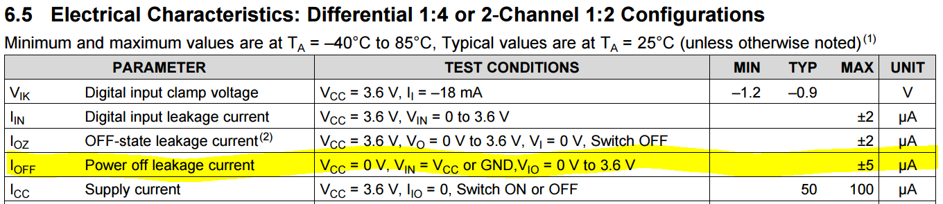
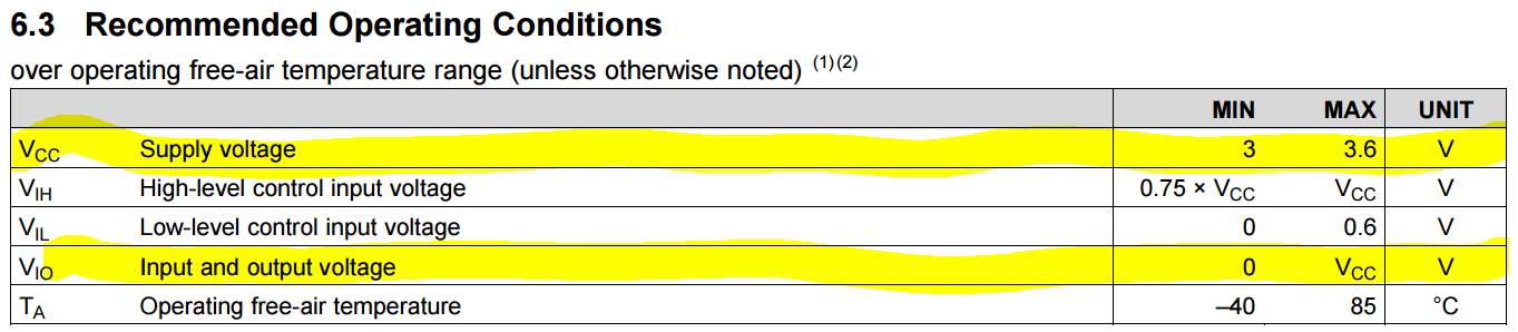
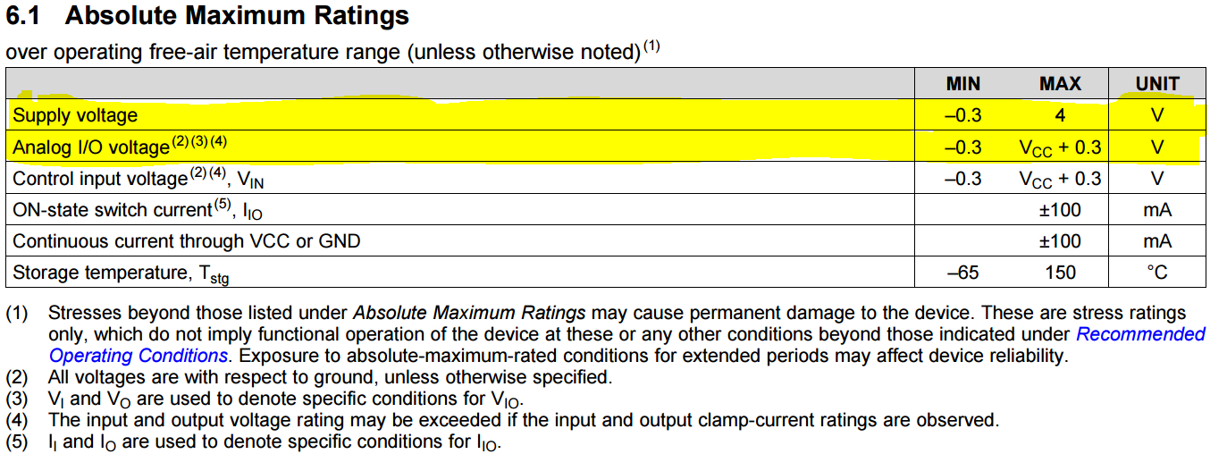
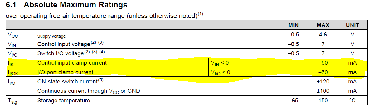
With this device, what happens when Vcc=0V but there is a 5V signal on the input?  Are they effectively high impedance?  I noticed a spec in the datasheet for Fail-Safe protection and I was wondering.

Thanks,

Kareem

  • Hi Kareem,

    The Fail-Safe (IOFF) protection you are talking about is shown:


    This is stating that if Vcc = 0V your VIO can range from 0V to 3.6V and will have a max leakage current of ±5uA.

    However, I would pay close attention to the 5V signal on the input you mentioned. The recommended operation conditions specify the input/output voltage to not go above Vcc which has a recommended Max of 3.6V.


    Additionally, we cannot guarantee performance in the electrical specifications table outside of the recommended operation conditions. The 5V signal you mentioned is even above the Abs. Max ratings of 4V for Vcc and 4.3V for IO voltages and can cause permanent damage to the device and or affect device reliability.


    I have also linked to an old E2E post to calculate the impedance.


  • Thanks for the support.

    Regards,
    Kareem
  • Dakotah,

    There is also a note in the datasheet (subscript 4 in the last picture you sent) which mentions the voltages can exceed the recommended limits as long as the diode current stays below some clamp current limit. While this is unspecified in this datasheet, other parts in the family specify that clamp current at 50mA.

    It sounds like the high impedance of the pins in this case refers only to voltages within the operating range of 0-3.6V. At voltages above or below that, can I assume that the clamp diodes come into play, just as when the part is powered?

    It would help if I could see a schematic of the front end of the part – is anything like that available?

    Regards,
    Kareem
  • Kareem,

    As you mentioned, other devices specify the clamp current rating for the device. Unfortunately, any values specified in other datasheets should not be used as design parameters for your current device as they may differ.

    The schematic of the part is proprietary information and can not be provided. We will look into updating the datasheet values by adding this to our backlog and address it as the business case warrants.

    Additionally, the abs. max table shown is for the TS3USB221.

     Make sure to pay close attention to the values provided. The Ik current max is at -50mA. And the  Vin voltage is specd at Vin < 0. What this is saying is that the clamping diode from Vin to GND will kick in and clamp negative voltages up to that -50mA max. This does not specify a clamping diode to Vcc. This may help while looking into future parts.