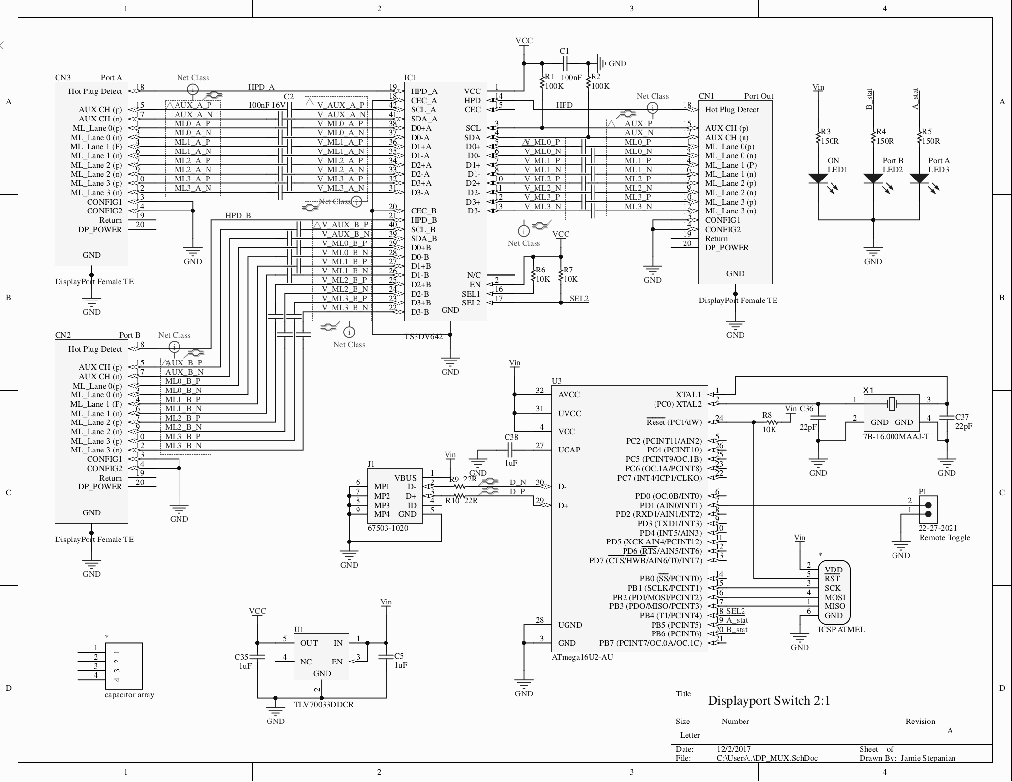
I'm currently prototyping a KVM with the TS3DV642 differential 2:1/1:2 MUX. It's intended to switch between two DisplayPort connector inputs out to one connector.
My question is, how should this connection be biased and ac coupled?
The datasheet specifies a need for around 1V bias conditions on the input, due to the FETs not being suitable for rapid negative swings. The following is their application note diagram for usage in a notebook embedded on the same board as the graphics card.
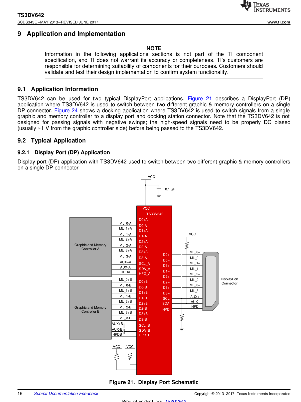
Above they have the convenience of making use of the DisplayPort biasing conditions before the graphics card ad couples the output (something a KVM can't leverage, as an external peripheral between source and sink connections!)
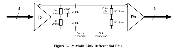
Bellow is the DisplayPort spec for the MainLink and AUX lines.

In my PCB design, I assumed that I could omit any ac coupling capacitors, and make use of the sink device biasing for MainLink connections (Vbias = 2V), and the source device biasing for AUX. This doesn't seem to work, and I don't have a +1GHz scope lying around to debug the board. I'm certain the differential signaling is properly laid out (intra/inter-pair skew is within spec, ground plane is unbroken, proper trace widths, etc..). I'm getting no signal out to the monitor (black screen on both inputs).
How would one properly bias this chip to use it as a KVM? Are there other issues that might make the implementation fail?