This thread has been locked.

If you have a related question, please click the "Ask a related question" button in the top right corner. The newly created question will be automatically linked to this question.

SN74CBTLV3383: Data corruption on A1-B2 path

Part Number: SN74CBTLV3383

Hi,

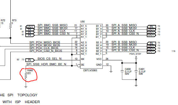
See the schematic excerpt below for reference.

Data corruption is occurring on the A1-B2 path when A1 is connected to B2 and A2 is connected to B1.

  • Simple burst reads will yield bad bits, but on re-read correct can be recovered
  • Issue manifests as fail to boot (cannot read BIOS) or fail to update (cannot correctly program BIOS)
  • Device is being used to access flash
  • There does not appear to be any temperature dependency (issue occurred at 25C).
  • PCH and BMC are both masters and are both on "A" side
    • BMC access is at 20MHz nominal and sometimes up to 25MHz
    • PCH access is at 30MHz nominal and sometimes up to 40MHz
  • Vil/Vih issues does not seem to be a possible reason for failure.
    • two vendors of SPI flash is used, both are expected to have same Vih / Vil

Two experiments tested thus far:

  1. When stopping data transmission on the A2-B1 path, the problem goes away. This reliable stops the failure
Changing the 221 ohm pulldown resistor to 0ohm on /BE seemed to resolve the issue
  1. They will switch back to 221 ohm to see if the issue returns
  • Note: There was a reported case where the "issue fixed itself" after they simply tried probing the lines

  • Formatting issue on the last paragraph:

    Two experiments tested thus far:

    1. When stopping data transmission on the A2-B1 path, the problem goes away. This reliably stops the failure
    2. Changing the 221 ohm pulldown resistor to 0ohm on /BE seemed to resolve the issue
    a. They will switch back to 221 ohm to see if the issue returns
    b. Note: There was a reported case where the "issue fixed itself" after they simply tried probing the lines
  • Cassidy,  

    This device has a bandwidth of 200MHz so you shouldn't be seeing too much attenuation with your 40MHz signals so I agree it might not be a vih/vil issue on the signal path to the flash memory.

    The vih and vil on the OE pins for this device with Vcc = 3.3 V are 2 V and 0.8 V respectively.

    In the experiments tested thus far:

    1. Stopping the data transmission makes the problem go away?  Are you thinking that there is a cross talk issue?  Do you have scope plots of the data on A1 and B1 and A2 and B2 in the failing and non failing case?  You can also try removing the IC from the board and short the signal path to see if the issue goes away.  This will help determine if the cross talk is through the IC or through the board.

    2. You have a very strong pull down resistor and you change it to a stronger one pulling it to ground through 0ohms that will always enable the switch.  It seems odd to me that changing this pull down resistor by 220 ohms solves the issue.  How repeatable is this?  Do you have a scope shot seeing what voltage is on this node in both cases? 

    A) How many boards is this failing signature seen? 

    B) Does replacing the IC solve the issue?  Does the removed device cause a good board to fail?

    Thank you,

    Adam   

  • We determined that the /BE pin was not having an effect on failure rate.

    However, we know that crosstalk in the IC is in someway causing the failure (if we blue-wire the connections we don't get failures).  Capturing the precise moment when failure occurs has been difficult, the times we have caught failure it appears that the flash is actually clocking out incorrect data (however tests showed this is likely because an error occurred during a write operation). After further tests we saw that some boards experienced read failures while others experienced write failures. Write failures appear to occur far more frequently than read failures.

    The flash IC (which is connected to the B side of the switch) has a very strong drive strength/fast rising edge and when multiple lines rising edges are synced they cause a significant amount of crosstalk. Tying pins 3 & 4 of the switch to GND via 0ohms has eliminated all errors in all cases thus far. We suspect that tying those pins to GND helps attenuate some of the crosstalk in their system. We are also recommending that the series resistors on the communication lines be increased to help slow down the flash's rising edge.

  • I should add: a previous flash was used successfully in another design. And that flash was using a different (and slower) process. Efforts are currently underway to determine the actual differences between the flash parts and how that might affect the switch and the design overall.
  • Cassidy,

    I'm glad you found out that grounding pins 3&4 eliminated the errors. We do recommend that you terminate unused pins to ground vs leaving them floating for best signal integrity performance.

    Thank you,
    Adam