


Hi,team,
I have one question about SN74CBTLV3125.
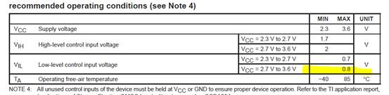
What is the minimum voltage of VIL? Does it mean if voltage is <0.8V, the output is ensured LOW?
Only maximum value is marked in datasheet.
Thanks.
Johnny
Hi,team,
I have one question about SN74CBTLV3125.
What is the minimum voltage of VIL? Does it mean if voltage is <0.8V, the output is ensured LOW?
Only maximum value is marked in datasheet.
Thanks.
Johnny


