This thread has been locked.

If you have a related question, please click the "Ask a related question" button in the top right corner. The newly created question will be automatically linked to this question.

Reason for distorted waveform at the output of the gate drive IC.

Expert 1140 points
Other Parts Discussed in Thread: UCC27524A, UCC27531, UCC27511A, UCC27517A

hai,

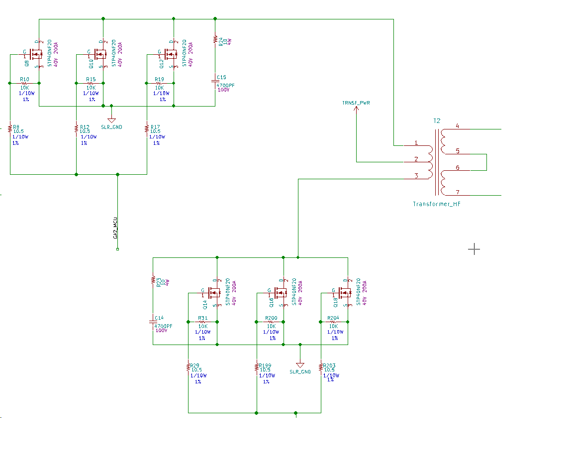
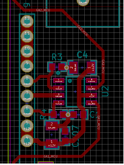
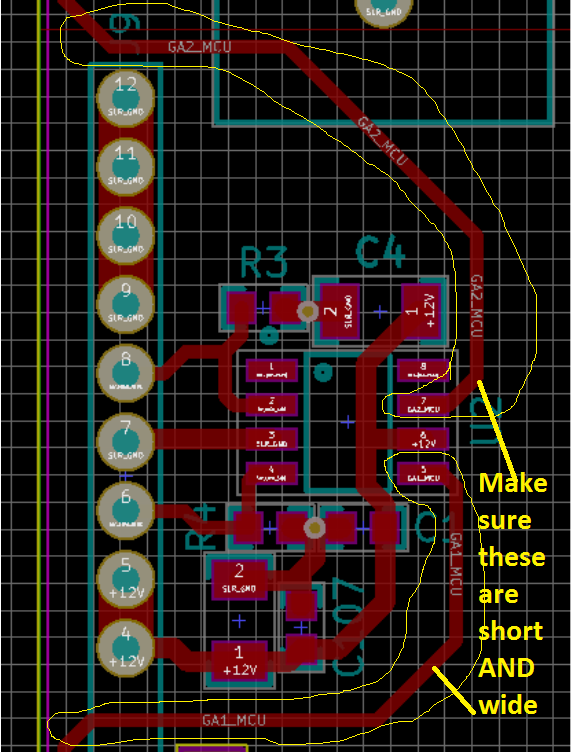
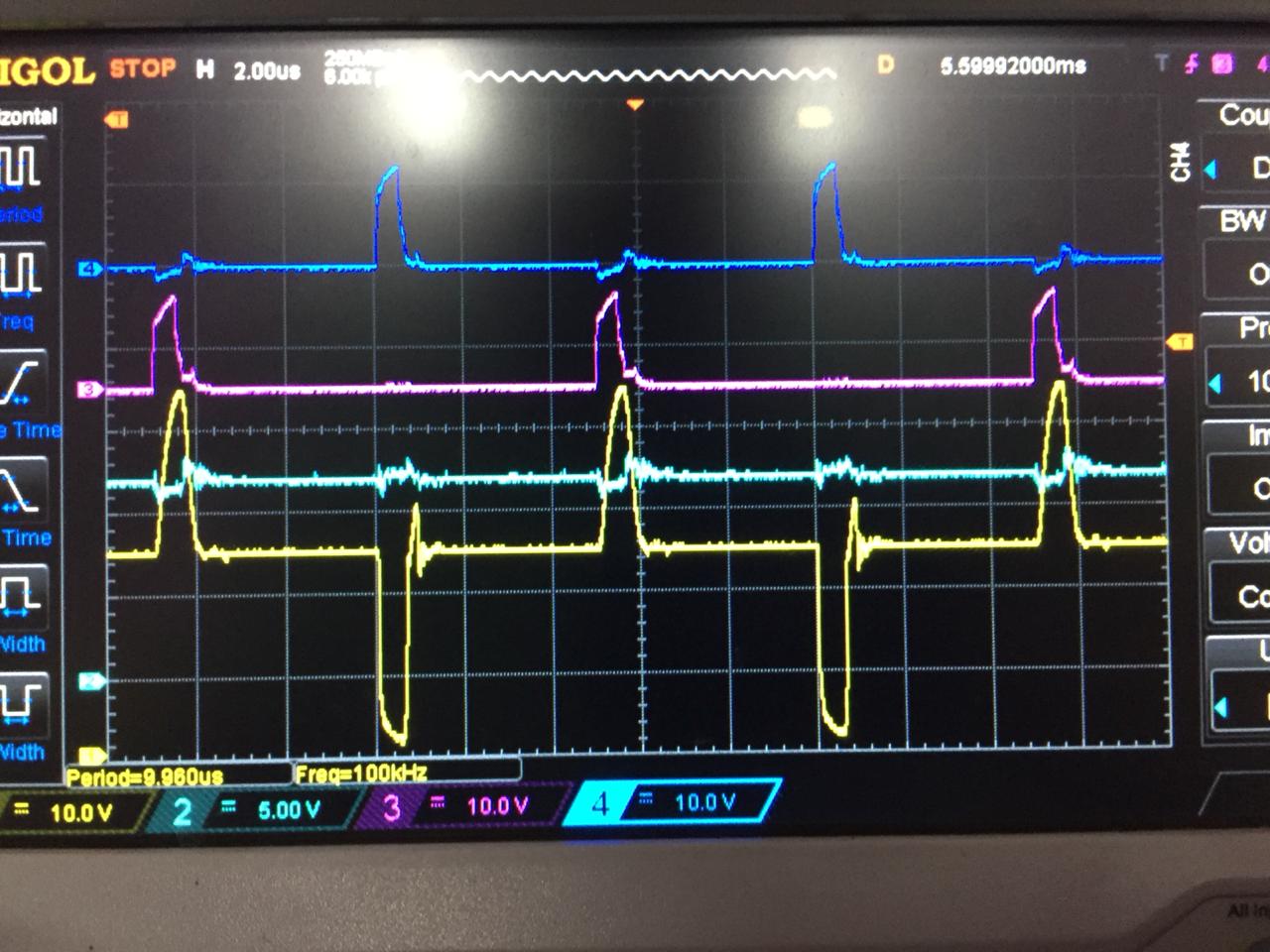
i am presently designing an inverter using pushpull topology.I am using IXX4427NTR as my gate driver.i have mosfets attached on two coils of my push pull transformer driving my configuration.I am giving square pulses at the input of the gate driver but happen to see that the waveform is distorted.What could be the reason for the shape change of the input waveform.I have routed the board in such a way that , the trace connects all mosfets on a single line but the shape of the gate signals varies from nearest mosfet to the mosfet at the far end why is that so?

  • Hello Amal, 

      I am not seeing any Texas Instruments devices in the design or referenced in your description. Please provide more detailed information and I'm sure we can come up with an appropriate TI solution. 

    Regards,

    ~Leonard 

  • Hai,
    It's actually true that I am not using any ti devices but I am actually in search of non inverting type gate drivers having two channels capable of driving my system.Could you suggest any ti products inreplacement for same.I doubt the working of gate driver which seem to distort the gate signal
  • Hi Amal,

    My name is Mamadou Diallo, I am an applications engineer supporting low-side drivers in the High Power Drivers group.

    UCC27524A to drive pushpull transformers, this device is p2p compatible with the IR4427 i believe you referenced in your previous post. The EN pins (Pins 1 and 8) are internally pulled up to VDD therefore may be left floating.

    As a first step, I would recommend replacing that device with UCC27524A and if you observe further waveform distortions, please let us know (with some scopeshots if possible) in order to help debug the root cause.

    Additionally, you may find more dual-low side drivers on our portfolio page on the link below:

    ti.com/gatedrivers.

    Please let us know if you have further trouble with your circuit once you replace the device with UCC27524A or press the button if it resolves the problem.

    Thanks.

    Regards,

    -Mamadou

  • May I also suggest these gate drive topics for your consideration.

    Power Tips: A simple circuit for driving gate-drive transformers,


    Fundamentals of MOSFET and IGBT Gate Driver Circuits

    Design And Application Guide for High Speed MOSFET Gate Drive Circuits

    Using TI gate drivers along with following TI application material will lead to a robust design.

  • Hai,

    I have purchased the gate driver ic UCC27524A and am yet to test with it.I have a major doubt regarding the gate waveform.I found that ,without the mosfets mounted ,i have a clear square waveform at the gate terminal of the MOSFET.Should i doubt the inability of the driver to handle such a load.Different from my design i am using only one mosfet at each half of the transformer. I am presently driving a single SUG90090E-GE3 at two individual half's (instead of three FETS)using  the driver IX4427NTR.Will the Cgd and Cgs of the mosfet be the reason for this problem?

  • Hi Amal,

    Thanks for purchasing UCC27524A.

    Looking at SUG90090E-GE3 datasheet, this device has typical gate charge of 86nC which would require strong driver to supply consistent gate (source/sink sink) current to efficiently charge/discharge the gate and drain capacitors given that gate charge is a the produdct of average gate current and time required.
    UCC27524A has a 5A source/sink current capability which would be better fit for such a heavy load especially if you plan on using the 3-parallel FETs.

    As a sanity check, you may consider placing a FET with lower gate charge to see if you're still observing the distortion.

    Also, please share waveforms of the distorted signal along with the input signal.

    Thanks.

    Regards,

    -Mamadou
  • Hai,

    since i am moving on with new revision of my board, do you have any routing suggestions to be implemented for the gate driver routing.Should i place the series resistor near or far from the driver? Should i place them at the mosfet or the driver side? have attached the pic of my present design.please see the routing implemented

  • Hi Amal,

    Your input stage seems good but it is important to prioritize the power stage(SHORT wide traces from driver output to FETs).

    Here are general guidelines for an optimized layout to minimize the effects of parasitics in the gate drive portion:

    1- Check turn-on and turn-off current loop path (driver, power MOSFET and VDD bypass capacitor) and ensure this loop is minimized(as small as possible) in order to reduce stray inductance

    1a- Check location of the bypass capacitors and ensure that they are placed very close to the driver’s VDD pin ( I recommend 2 Low-ESR and low-ESL bypass caps:  >=1uF and a second usually 0.1uF to support the high peak currents required to turn-on the power FETs).

    1b- Check location of the gate resistor AND MOSFETs and ensure that they are placed very close to the driver’s output pin to reduce PCB trace length and minimize loop inductance (this step is related to next step). I see in your layout long PCB traces from OUTA and OUTB which will introduce significant parasitic inductance in turn-on/off path.

    2- Check location of power traces and signal traces such as output and input signals and ensure they are separated

    Additionally, Section 11 from the driver's datasheet gives supplementary guidelines on best layout practices from a gate driver perspective.

    Please let us know if you have further questions.

    Regards,

    -Mamadou

  • hai,

    what is the minimum supply required for UCC27524A driver?How much current would it draw or consume when driving a load of 129nC Driver.It is unfortunate to say that still my Gate drive signals are distorted of before even after changing it from IX4427NTR TO UCC27524A.What could be other possible reasons behind the distorted waveform which appears at the gate after the fet is being mounted?

    Presently i am using only two fets,which means each channel is being driven by a mosfet each(SUG90090E).What could be other possible reasons behind this issue?

  • Hi Amal,

    Have you optmized your layout? When using gate drivers, layout is critical! You have to prioritize the power stage and especially distance between the driver's output stage and the MOSFETs. OUTA and OUTB seem connected to the FETs with very long PCB traces which will introduce significant parasitic inductance at the gate compromising the switching of the FETs. You need the MOSFETs connected as close as possible to the driver's output with SHORT, WIDE traces.


    Regards, 

    -Mamadou

  • Hi Mamadou,

    I have attached the waveform which I obtained while testing with the fets.
    Dark blue and pink channels represent the gates of mosfet.Yellow is drain of mosfet which burned after two or three cycles of testing.Light blue is 12V power supply.
    I really doubt whether the mosfets are switching on properly.I also feel that my power supply is getting loaded.its basically a 3 amps rated power supply.Do you have any assumptions based on these waveforms?

  • Amal,

    Beside the layout previously highlighted, here are couple of observations/suggestions:

    -It looks the signals at gates are taking quite a while to go high. You may reduce your gate resistors (currently at 10.5-Ohms) to help speed up the dv/dt at the gate.

    The tech note below from my colleague will help you choose the appropriate value. 

    You may also consider adding an anti-parallel diode (in parallel with your gate resistor) to help speed up the turn-off of the MOSFET and reduce the switching losses.

    -Additionally, there seems to be ringing on the VDD supply which could lead to further trouble down the road. If not already implemented, please ensure that the 2 bypass parallel caps shown on your layout are >=2uF and the second =0.1uF. to help filter noise on the supply and provide the peak current to turn-on/off the FETs effectively.

    Regards,

    -Mamadou

  • Hai Mamadou,

    How should I calculate the total current required by each channels to drive my mosfet.I happen to see the Fet SUG90090E Qg  Max to be 129nC. How Should I calculate the current required.I am driving my gate driver circuit by using a 3A power supply.Will it be sufficient to drive my fets. Actually maximum duty cycle is 0.45.Does the circuit need a supply more than 3Amps?

  • Hai Mamadou,

    What are your suggestions of using two separate gate drivers for two different channels?I am planning to place them right near the MOSFET.I can ensure shorter traces from OUPUT of the driver to the gate of the mosfet.Rerouting the present design would be difficult.We are planning for single channel drivers for each gate drive signal.What are your suggestions about this? If this design topology would not have much issues then could you please suggest me single channel drivers for my design?I will buy them right away and start testing with them.

  • Hi Amal,

    1. If you're considering switching to 2 separate gate drivers, remember you would be increasing board space and component count on your design.
    Having said that, we have many single channel low-side drivers including UCC27511A, UCC27517A and UCC27531. The difference is their output configuration (split output which helps when you need to optimize the turn-off of the FETs and the single Output) and the supply range (UCC27531 goes up 30V VDD) and drive current.
    You may find more devices on the link below:

    www.ti.com/.../products.html

    For an optimized layout, you may refer to EVMs or consult the layout guidelines section of our datasheets.

    2. Driving a MOSFET is essentially charging/discharging a capacitor therefore driving the MOSFETs will be similar to charging and discharging the capacitor. You can use Ig = C* dv/dt where Ig = gate current required to turn-on the FET, C = total capacitance and dv/dt = the desired transition time for the gate voltage to reach your drive voltage or VDD. You probably noticed that you cannot control the capacitance but you can control the the dv/dt by tuning the your gate resistor. Higher dv/dt will mean lower gate resistor value which will translate into higher gate current resulting in less switching losses on the FETs.
    Similarly, Ig = Qg / t_on/off is also a direct way to calculate knowing the total gate charge. Again t_on/off is controlled by your choice of gate resistor. However, too small of a gate resistor may cause overshoot resulting in EMI noise at the gate. So you have find your middle ground based on your need.

    3. Given that you have that much gate charge, a >4A/5A driver should be adequate to effectively turn-on/off the FET.

    Regards,

    -Mamadou