This thread has been locked.

If you have a related question, please click the "Ask a related question" button in the top right corner. The newly created question will be automatically linked to this question.

TIDA-00792: Why we need both discharge and charge protection FET in BMS ?

Part Number: TIDA-00792
Other Parts Discussed in Thread: TIDA-00449

Hi all,
I have two questions>>
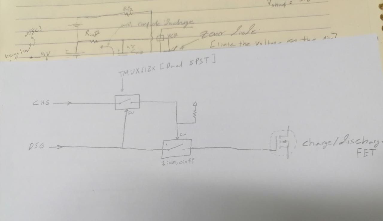
First, why we need both discharge and charge protection FET in BMS? Okay, we need both protection features but why they are separate? I think it's better to, kind of OR the two signals into one MOSFET! Right or I missed something? 

Second, I don't understand why we need the High-side FETs?like in TIDA-00792, so I read "bq769x0 3-series to 15-series cell battery monitor family for li-ion and phosphate applications". and find the following:
"High-side FETs enable continuous communication between a host
controller and the monitor, regardless of whether the FETs are on or off. This allows the controller to read critical
pack parameters despite safety faults, enabling the system to access pack conditions before allowing normal
operations to resume."

But using low-side FET as in TIDA-00449 I think I just take the ground(Of course before the FET) with the two SMBus lines! then how communication will be not continuous?

Help, please xD

Thanks in advance.

  • For the second question as I read in "bq769x0 Family Top 10 Design Considerations" find the following on page 13:

    "Communication with a battery over a ground referenced interface such as SMBus is typically connected to
    PACK-. When low side protection FETs are used, PACK- is disconnected and reference for the
    communication lines is lost. The.."

    So why it's "typically" connected to PACK- as in TIDA-00792 ? why not to BATT-? 

    And for the first question, I know you can say that for many systems the charge current is much lower than the discharge current so they can have separate path and different FET, but why in design like TIDA-00792 or TIDA-00449 the use the two FET even they share the same path as just two switches for the same path?

  • Hi Rashad,

    Thanks for the inquiry. I am the applications engineer for the FET product line and was not involved in these reference designs. I am going to pass this onto the battery gauge products team that did this design.

  • Hi John,

    Okay, Thanks a lot I am waiting.

  • Hi Rashad,

    A battery is typically expensive and both the user and supplier want it to last a long time for customer satisfaction.  If the battery reaches a condition where it should not be charged it may be allowed to discharge.  If the battery is fully discharged it may be allowed to charge.  A single control such as a relay blocking both charge and discharge would prevent these actions without additional consideration.  It would be possible to measure the battery voltage, pack terminal voltage and other parameters to determine if it was safe to close the relay, some systems do that but it is not the technique which has commonly been used in smaller batteries.

    Requirements for battery terminal access varies with the industry and equipment where used.  In some systems it is considered OK to have both PACK- and BAT- come out of the battery is acceptable because none of the contacts are available to the user. Cost sensitive designers will not want to pay for the extra contact. In some systems for consumers where the battery is removable having a low side switched load (PACK-) with BAT- always available is unacceptable because the customer might short from PACK+ to BAT- and the battery would not be able to react.  A 2 terminal fuse might prevent prolonged high current but would not prevent slow discharge. Discharge and possible damage by connecting PACK+ to the communication interface lines could also be a concern. A discharge from PACK+ to BAT- would bypass the current sense resistor and the battery would be unaware of current and unable to react to current events.  High side switching prevents over discharge to BAT- or communication lines.  An isolated communication bus is also a solution and is sometimes required for the system, but this involves more components, area, power, and cost than many designers desire so it is usually only used when required.

    Check your system requirements and use an approach suitable for your design.

  • Hi WM5295,

    Thank you very much! now the second question is very clear.
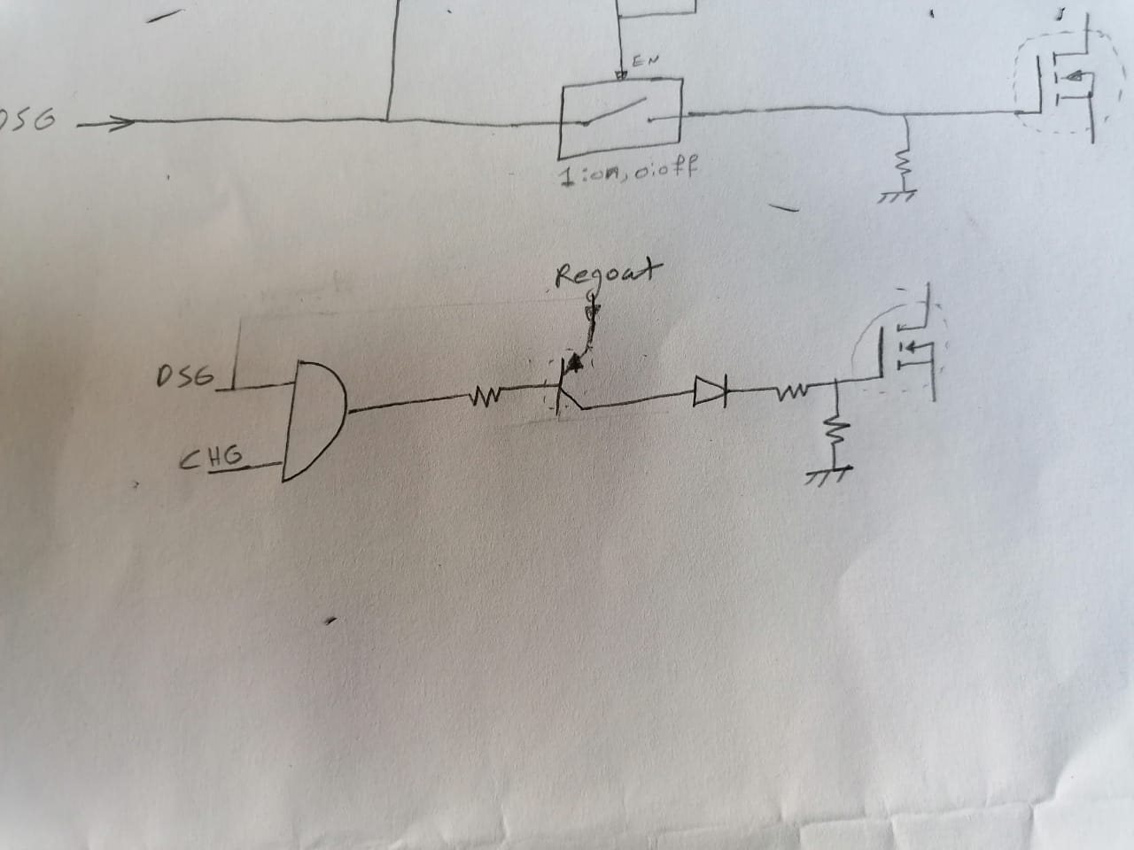
    But I don't think that the first question is answered well or maybe I don't get the point since I know the situation where we need to use both discharge and charge protection FET, but I don't understand the need of them in common charge/discharge path? as in  TIDA-00792 and TIDA-00449. or we just forced to use them like this because of the behavior of the chip itself? "Table 1. CHG, DSG Response Under Various System Events" in the datasheet. If just forced to use them like this, so this idea can help or it's not a good and practical one(as in the picture below, with pull-down Resistor on FET gate)?

    Best Regards,

    Rashad Shubita

  • Hi,

    Maybe something like this is better, right?

  • Hi Rashad,

    I'm uncertain of your complete topology, that is for you to work out.  Remember that a FET blocks current in only one direction, in the other direction it is a diode. So a single FET can not prevent both charge and discharge.  A pair of FETs with the sources connected can block current in both directions and provide a single control if appropriate.  FETs connected with a common drain will typically need separate control lines such as the FETs shown in TIDA-00792.. 

    In your first drawing as amended in the second, it is the resistor on the gate of the final FET which turns it off if CHG goes low.  In your second drawing remember that REGOUT is a low voltage (varies with the part number selected) while CHG and DSG are about 12V if in regulation.  Be sure to keep the logic and the PNP safe.  It does not leave you much gate voltage for the FET shown.  Again realize it is the resistor shown to GND which turns off the FET.

    Think through what you plan to do.  A simulator like http://www.ti.com/tool/TINA-TI or others available in industry may be helpful to understand FET switching, but be cautious of the transistor models, some show high leakage, you still need to test to validate your circuit. 

  • Hi WM5295,

    Again thank you very much! now everything is clear to me. I really forget the body diode in FET.  Nice explanation thanks!. Can you give me a good reference where I can understand FET switching really good? and all consideration I need to take, also FET driver? 

  • Hi Rashad,

    Check your favorite FET supplier's website for technical articles on FETs, or search on the internet for FET information.  For drivers look at http://www.ti.com/lit/slua618 or other information at http://www.ti.com/gatedrivers