This thread has been locked.

If you have a related question, please click the "Ask a related question" button in the top right corner. The newly created question will be automatically linked to this question.

WEBENCH® Tools/LM5122: Obtaining more power from LM5122 48V Boost

Part Number: LM5122
Other Parts Discussed in Thread: LM5170

Tool/software: WEBENCH® Design Tools

Looking to design 12V - 48V Boost converter using the LM5122MH/NOPB. The current needs to be 20A max but I get error from Webench stating current exceeds limit. Is there a way around this in simulation so I can get the design I need? I specified my range of input voltages between 20V and 30V. I am planning to run two 350W electric motors using this boost converter. Thanks.

  • Hi Amar,

    Thanks for reporting this, we're able to reproduce this and working on fixing it. We will keep you posted on the proceedings.

    Regards,

    Vishwanath

  • Hi Amar,

    This is a high current design. Single FET solution may not be sufficient for these input/output conditions. We're working on implementing parallel FET and Ideal Fet solutions. These changes may take till mid December for them to be released on ti.com

    Rergards,

    Vishwanath

  • I made a mistake in my first question. For the 48V boost the input voltages are 20V - 30V and output voltage is 48V at 20A

    For 24V Boost, input voltages are 10V - 20V and output voltage is 24V at 40A.

    My sincerest apologies.

    Thanks

  • Hi Amar,

    We're still working on this.

    Regards,

    Vishwanath

  • Hi Amar,

    Thanks for your patience. We will let you know once the Ideal and Parallel FET support for LM5122 is enabled.

    Best Regards,

    Harish

  • No Problem. Will there be available a full board layout and bill of materials list in TI Webench because that is what I`m looking for. Will I be able to access before 12/15? I need this soon.

    Also, how many layers will the board be?

    Thanks

  • Hi Amar,

    We are working to provide WEBENCH design support for high output power / load for LM5122.

    Kindly note that we might end up with either Ideal/Custom FET in case WEBENCH is unable to find suitable parallel FETs.

    Below is the current status for your conditions

    1. Vin=20V - 30V, Vout=48V at 20A

    We are able to get parallel FET for this design. Also inductor is resulting in custom component since high current rating inductors are not present in WEBENCH database.

    2. Vin=10V - 20V, Vout=24V at 40A

    Currently the device max Iout is limited to 35A in WEBENCH. So we are checking with product expert if this limit can be increased.

    Even if we enable high Iout design, we will most likely end up with Ideal FET for this design. Also inductor is resulting in custom component 

    Regarding PCB/Board, currently WEBENCH infrastructure doesn't support for Ideal/Parallel FET.

    Any changes that we do will mostly be available on ti.com by 20Dec2019. Kindly let me know in case of any queries.

    Thanks & Regards,

    Harish

  • For the 24V Boost, I would be fine with max output current of 35A if I would be able to export the board design to altium. 

    If an inductor is custom can it be replaced by a through-hole footprint where I can install my own custom inductor?

    Thank you for the update,

    Regards,

  • Hi Amar,

    For custom inductors and Ideal FET, you can download Altium files from WEBENCH and use inductor from local library.

    Thanks & Regards,

    Harish

  • Hi Amar,

    We have enabled the ideal FET for this device and changes will be available on ti.com by end of next week.

    Thanks & Regards,

    Praveen 

  • Hi Amar,

    You should now be able to create designs for below conditions on WEBENCH for LM5122.

    1. Vin=20V - 30V, Vout=48V at 20A

    2. Vin=10V - 20V, Vout=24V at 35A

    Kindly let us know in case you need any help.

    Thanks & Regards,

    Harish

  • I was having difficulty finding a suitable high current inductor. Would it be okay if I used this? https://www.mouser.com/ProductDetail/Vishay-Dale/IHXL2000VZEB2R2M5A?qs=AQlKX63v8RvThbc%252BB5a6jw%3D%3D

    Its a 2.2 uH inductor unlike the 1 uH specified.

    If I can use it, is it possible for you give me the option of selecting this inductor as an alternate part?

    Thank you so much for your help

  • Hi Amar,

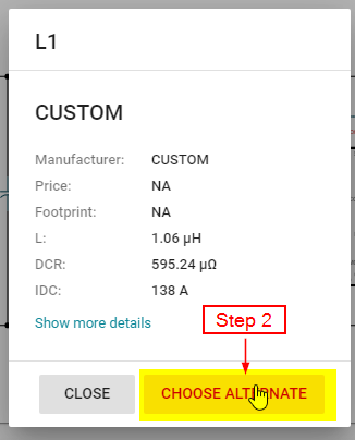
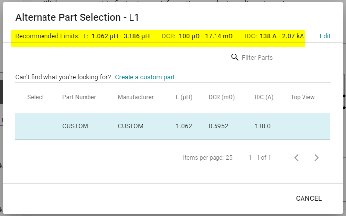
    WEBENCH usually provides recommended range for each of the BOM components. You can check the recommended range by clicking on particular BOM in WEBENCH schematic and click on "Choose Alternate" button. Please follow steps mentioned in below images to verify recommended range for inductor.

    You can use "Edit" option to edit the "Recommended Limits". However WEBENCH database doesn't have IHXL2000VZEB2R2M5A inductor, so you will not be able to select this inductor.

    As per WEBENCH recommended range, 2.2uH inductor can still be used. The only spec that IHXL2000VZEB2R2M5A inductor violates is IDC (A) rating.

    IHXL2000VZEB2R2M5A has IDC rating of 125A whereas WEBENCH recommends minimum of 138A. However 125A rating inductor should be fine for [Vin=10V - 20V, Vout=24V at 35A] condition  since WEBENCH adds some margin for more reliable designs.

    Before proceeding with your application design, we would strongly recommend you to verify the results on board.

    Thanks & Regards,

    Harish

  • Ok. What do you mean by verify results on board? Breadboard?

    Regards,

  • Hi Amar,

    I meant to test on one PCB board before you finalize / go for mass production for your application.

    Thanks & Regards,

    Harish

  • Of course.

    What are these resistors for in the board layout? Can I just short these pads since they do not appear in the schematic?

    I also noticed these vias which I think I can take out and connect the traces directly to the sense resistor.

    Thanks

  • Hi Amar,

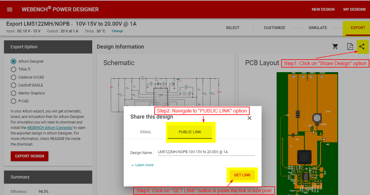
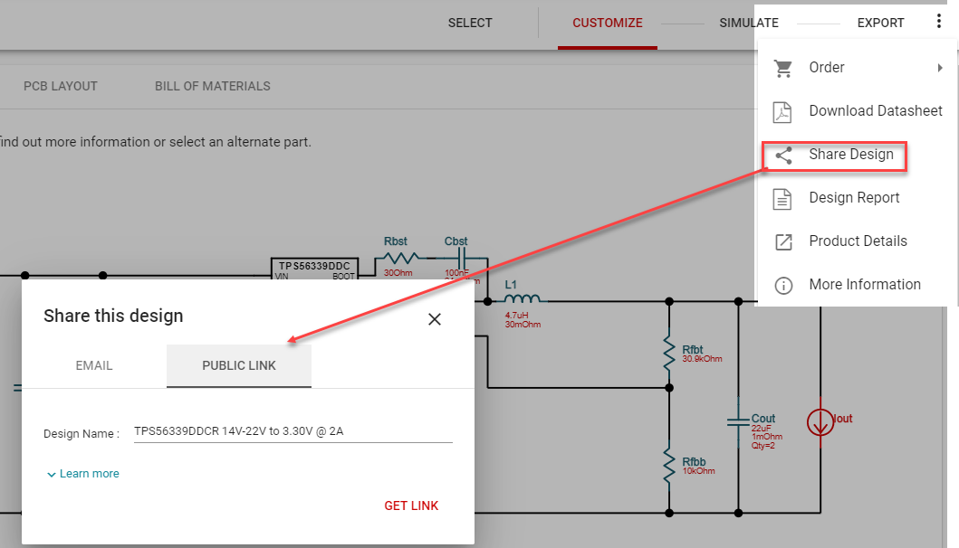
    Could you please share your design by following steps mentioned in below image to help you better ?

    Thanks & Regards,

    Harish

  • I sent the link. Can you also check if the 21 output capcitors (120uF) is correct? Instead of 21 Caps I am planning to use 3 1000uF capacitors.

    Thanks

  • Hi Amar,

    Currently, the resistors Rcsfn and Rcsfp are not present on the WEBENCH schematic. We will update the PCB board accordingly. Since CSN and CSP are high impedance and noise-sensitive signals it is recommended to connect these traces to Rsense resistor using Vias instead of connecting to top layer polygons.

    WEBENCH database has a limited number of capacitors that satisfy the VDC, Irms and ESR requirements for the above condition and hence 21 output capacitors(120uF*21) are added in the parallel on WEBENCH schematic.

    Thanks & Regards,
    Praveen 

  • Hi Amar,

    We will update the PCB board. We will let you know once the fix is available on.ti.com. 

    Thanks & Regards,

    Praveen

  • Ok please let me know soon. What values are the resistors Rcsfn and Rcsfp? Send me the link please

    Thanks

  • Hi Amar,

    The WEBENCH schematic does not have the Rcsfn and Rcsfp resistors. We will remove the same from the PCB board.

    Thanks & Regards,
    Praveen 

  • Ok, I already removed the pads myself.

    What Vgs voltage is applied to each MOSFET to turn it on? I am looking for a high power MOSFET and needed to make sure I chose the correct one with right Vgs.

    I was not able to look at alternate MOSFET`s specifications like for the inductor in WEBENCH power designer.

    Would this MOSFET be good to use IRFB4115PBF? Do you have any recomendations?

    Also, is there a way for you to enable the efficiency calculation in webench? I needed to choose an appropriate switching frequency.

    Thanks

  • I changed the switching frequency to 172.084 because it suited my inductor value, but the Cvcc capacitor is custom. I needed assistance choosing a custom value.

    Also, is Coutx(44uF) needed? Sorry for asking so many questions

    Thanks!

  • Hi Amar,

    The Gate to source voltage applied to both HIgh and low MOSFETs is equal to VCC voltage(7.6V). WEBENCH does not find any suitable FET for this condition and hence ideal FET is being selected on WEBENCH. Efficiency calculation & alternate MOSFETs list is not shown on WEBENCH for ideal FET. The IRFB4115PBF FET has higher power dissipation and it violates the maximum junction temperature of FET for this condition. 

    Kindly select the 47uF,16V Cvcc capacitor. The recommended range of Coutx is 40uF-50uF 34V.

    Thanks  & Regards,
    Praveen 

  • Hello, 

    We have tried the 24V boost circuit, designed at 172.084kHz, and it is setting the output voltage to 24V with no load connected. When attaching a resitive load however, the voltage drops to 17V or so. What could be the reason for this? What components do we need to check?

    Thanks,

  • Hi Amar,

    Please let us know more details on your input/output conditions and schematic or please create a WEBENCH design for your conditions and share it with us as shown below. This will help us to understand & debug the issue.

    Thanks & Regards,
    Praveen

  • I am using two 3.3 uH inductors in parallel, is the inductance too low?

  • Hi Amar,

    Please let us know the below queries on your design.

    1. The WEBENCH design you have shared have two ideal MOSFETs. Could you please let us know which FETs are being used on your board design.

    2. Do schematic and BOM components match with WEBENCH design?. If not please share the schematic and BOM components.

    3. We have simulated the above WEBENCH design and the output voltage is settling to the expected value. We will forward your query to experts to review board design.

    Thanks & Regards,
    Praveen

  • Hi Amar and Praveen,

    This is from the BSC product line. We own the LM5122 IC, and we just noticed this thread.   

    I am afraid a single LM5122 cannot support 48V @20A. Your targeted application is up to about 1000W and the 3A driver of the LM5122 is not strong enough.   The maximum power that we get with the LM5122 for similar applications is about 200 to 250W in with a single LM5122.  Higher power require paralleling more LM5122 in multi phase configuration.   There are reference designs which you can find at the following webpage.

    https://www.ti.com/product/LM5122/toolssoftware

    A more suitable device to support such high power is the LM5170 (https://www.ti.com/product/LM5170), which is a dual phase controller. The driver is much stronger and a single device can support 1000W.  The condition is that you need to find a suitable inductor to support 500W, so you can do 100W in dual phases with a single LM5170 IC. If not, you may consider three or four phases with two LM5170 in parallel configuration.  

    You can first try the standard EVM which is limited to about 700W in dual phase, mainly limited by the inductor not by the LM5170 IC itself. If you can swap the onboard inductors with a larger, higher current rating one, you can test for higher power.  Remember to increase the resistor at IPK pin to open up the cycle by cycle current limit threshold when you use larger inductors, to allow higher current.

    Thanks,

    Youhao Xi, Applications Engineering 

  • Hello,

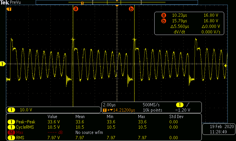
    Sorry for late response. I was able to get the 24V boost to work but only 75% efficient. We are seeing "ringing" at gates of mosfets which may be causing my low efficiency. Would I design a resistor-capacitor snubber circuit to eliminate this and how?

    Thank you so much,

  • Hi Amar,

    The waveform look like the switch node voltage.  It shows your circuit is running in deep DCM.  What is your max load level, and what is the load for this measurement?

    If it is measured under full load, then your inductor is too small.  You should increase the inductor value.   In DCM, the rms current under full load can be excessive causing a lot of switching and conduction losses.  Please follow the datasheet design examples to chose the right inductor value.

    Thanks,

    Youhao

  • No it was not measured under full load. Can someone suggest how to add snubbers?

    Thanks

  • Hi Amar,

    Not sure why you are considering the snubber.  If you add, it is usually placed across the high side FET. 

    If you are trying to smooth out the ringing shown in above scope picture of your measurement, you may leave it alone because it is typical DCM resonance, a resonance between the main power inductor and the MOSFET Coss.  You should consider to increase the inductor value to shorten the duration of the resonance. 

    If you set the circuit to FPWM, you should not see such riging.

    Thanks,

    Youhao

  • We now believe the issue is caused by our MOSFETS https://www.vishay.com/docs/76843/sqp90142e.pdf

    The VGS is 10V and our LM5122 has VCC that can only supply upto 7.6V. Is it okay to use a power supply to initially supply 10V to Vcc pin as shown in the datasheet below?

    Thanks,

  • HI Amar,

    First, why do you choose a 200V FET while 100V FET can do the job?  However, I don't think the problem discussed previously is related to the MOSFET. Your FET's Vth is only 4V, so the 7V driver can successfully drive it.  Like said, the ringing tail on the switch node voltage waveform is not a problem at all, and it is natural and normal in DCM.  You will need to change your inductor to operate the circuit in CCM if you don't like the ringing tail. 

    Anyway, yes you can supply an external supply to VCC like in above figure, and a higher driver voltage will strengthen the driver and you may see efficiency improvement.

    Thanks,

    Youhao

  • How much should I increase the inductance by? The ringing is making my boost 75% efficient.

    Regards,

  • Hi Amar,

    Use the following equations to determine the inductance, which will keep you in CCM above 30% rated load:

    Vin= (your normal Vin)

    Vout= (your desired output voltage)

    D=(Vout-Vin)/Vout   

    Then, the inductance should satisfy the following:

    L> (D x Vin) ^2 /(2 x Fsw x 0.3 x Po)

    Where Fsw is your switching frequency and Po is your full load power.

    Thanks

    Youhao