This thread has been locked.

If you have a related question, please click the "Ask a related question" button in the top right corner. The newly created question will be automatically linked to this question.

TIDA-01605: Protection in gate driver circuit.

Part Number: TIDA-01605
Other Parts Discussed in Thread: LM393, LMV762, ISO7721-Q1, ISO7721, TIDA-010054, UCC21530, ISO5452, UCC21750

Hello,

I have two points to discuss as follows,

1) Can we replace LMV762QMA with LM393 with 3k pullup resistor to make design of short circuit protection more viable? What are the other options to give short circuit protection because this IC will not work due to its wrong biasing according to datasheet of these ICs. I have read the thread in which Mr. Girish questioned about this and then searched LM393 for my design. Is it a viable option?

2) Using this tida01605 design for driving the SiC MOSFETs also needs to give voltage surge suppression circuit. If yes then how to implement miller clamp circuit in this TIDA? 

Thank you in advance

  • Hi Utsav,

    Yes, the LM393 could also work for this application. What specifically about the biasing of the LMV762 made it not work for your application/TIDA?

    Regards,

    Jonny

  • Utsav

    We have not received any response on this post in a while, so I will be closing the thread.  If you need further assistance, please feel free to reply and that will re-open the thread.

    Thanks

    Chuck

  • Hello to both of you (Mr. Jonny and Mr. Jonathan),

    I am working on isolated bridge DC/DC converters, in which each switch requires short circuit protection. In case we are using LMV762 with negative biasing, it may give negative output which will become input for ISO7721-Q1. And ISO7721 cannot take negative input. If I am wrong please correct me.

    Also, in this gate driver only one switch is protected, while in TIDA-010054 both the switches of one leg are protected with same two level turn off protection. Why is it so?

  • Utsav,

    By negative biasing, do you mean to say that the device is powered with a split supply such that output low would be equal to a negative voltage and output high would be equal to a positive voltage?

    I am not familiar with this TIDA design so allow me some time to review these design guides and get back to you on your second question.

    Regards,

    Jonny

  • Mr. Jonny,

    Yes.

    Please take your time.

    Thank you for having patience and solving my issues.

  • Utsav,

    Could you explain in greater detail what you are confused about in regards to one vs two switches being protected? Perhaps a picture of both schematics highlighting your concerns might help me identify what you are confused with.

    The circuitry is nearly identical, except that  TIDA-01605 doesn't explicitly include the circuitry providing the reference voltage for the inverting pin on the LMV762.

    Regards,

    Jonny

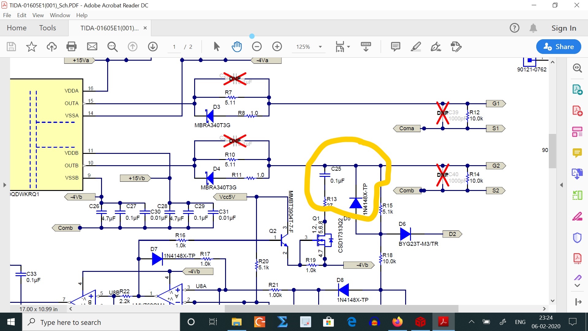
  • Attached picture is of TIDA 01605. In this design short circuit protection is given on G2 and S2, however in TIDA 010054 both the outputs viz. G1-S1 and G2-S2 are protected. What is the criteria to choose the two switch protection on one leg?

  • Hi Utsav,

    I'm unsure why in one document only one switch is protected and in the other both switches are protected. I specialize in responding to questions about comparators, but I feel that this question is more of a circuit design question about the dual channel gate driver.

    I am going to send this thread to the team that supports the gate driver in the TI designs document, UCC21530. Someone in the group that supports this product may have a more appropriate answer for you.

    Regards,

    Jonny

  • Hello Utsav,

    I am an applications engineer in the isolated gate drivers group. I agree with Jonny that it is not clear why the first TIDA you mention only provides the low-side SiC MOSFET protection circuit. I would assume this was done as a proof of concept, but not to show how it is implemented in the real system where you would need protection for both the low side and high side. The protection circuitry can be applied to both the high side and low side as in TIDA 010054. This is a good example to follow.

    Hope that answers your question!

    Regards,

    Audrey

  • Hello Audrey,

    Thank you for your clarification on high side and low side protection.

    Wide band gap (WBG) devices can pass current of very high magnitude through itself. Using this property, we can say that during short circuit condition in one leg there will be very high current in very less time. Can you please explain with some data of short circuit detection tests on WBG devices that this circuit will work?

  • Hi Utsav,

    Yes, short circuit detection must be very fast for WBG devices. Other than the waveforms and simulation data given in the two design guides, I do not have additional data. The circuit should be adjusted to fit your system requirements with respect to short circuit detection timing and threshold voltage and should be verified in your system environment. 

    The delay for DESAT detection is based on the time it takes for the capacitor to rise to the sense voltage (see page 9 of TIDA 01605). This can be adjusted with the value of C34. After this, there is a delay to transmit the signal across the isolation barrier to disable the driver. This is described on page 10. Then there is some delay before two level turn off is initiated.

    The total time to disable the driver should be shorter than your power switch's short circuit withstand time, so tuning this circuitry will take some design effort depending on the speed you need.

    We also offer isolated gate drivers with integrated DESAT detection and soft shutdown. See ISO5452 and UCC21750.

    Regards,

    Audrey