This thread has been locked.

If you have a related question, please click the "Ask a related question" button in the top right corner. The newly created question will be automatically linked to this question.

CC1190 reference design: Compatibility between 868MHz and 915MHz

Other Parts Discussed in Thread: CC1190

Hello,

We are going to add the CC1190 as a range extender in our low power wireless product. 

One of the requirements of this design is to maintain compatibility to work at two different frequencies: 868 MHz and 915 MHz. We have been looking for reference designs for the CC1190 to work at both and we found the following: 

--- For 868MHz: CC1120-CC1190EM 868MHz Reference Design swrr092 

--- For 915MHZ: CC1120-CC1190EM 915MHz Reference Design swrr089

Analysing these reference designs we have some questions about them: 

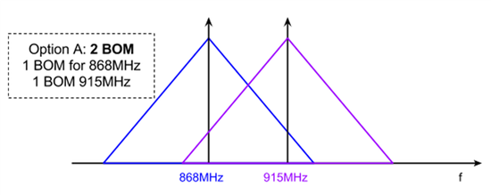
1. If we use these designs, we could have a single PCB (swrr092) for both frequencies and two BOM (one BOM for 868MHz and other for 915MHz). Is it correct to use the same layout for the two frequencies?

2. Is the swrr092 4-layer PCB construction compatible for both frequencies? Is it mandatory to use this PCB construction? Could we change any parameter to reduce fabrication cost?

With these features can we have a PCB that supports both frequencies and two BOM’s, one for each frequency, as shown in the following figure:


The design goal of the company is that if it is technologically possible, to have a unique product that works as optimally as possible for both 868MHz and 915MHz.

3. Is it possible to produce a single design to work at both frequencies?

If correct, what would be the best design choice to have a single product (same PCB and BOM)? Would it be feasible to center the bandwidth on the intermediate frequency? What would be the approximate value of losses in this case? Could this option be a problem for ETSI and FCC regulations?

 The following figure represent this option:

4. To enable this design option, we should adapt the design to fit that frequency. At schematic level of  CC1120-CC1190EM 868MHz Reference Design, do we have enough elements to adapt the network? Do Texas Instruments have a tool to calculate approximate values of the BOM, or should we fit the frequency at experimental level?

Thank you very much in advance,

Noa

  • 1) It is possible to use the 868 MHz layout for both 868 MHz and 915 MHz with different BOM.

    2) The same stack-up may be used for both frequencies. It is not mandatory to use this stack-up but I would recommend it.

       - If the distance between the signal layer and the ground layer is decreased the parasitics will increase changing the load and if the distance is increased the ground inductance will increase. Typically the ground connection to the die paddle on CC1190 is critical.

    - For this design short return paths are important and it's a lot easier to make a good ground with 4 layer design. Note also that the power plane is shielded by ground.

    Different layout is possible but with increased risk.

    3) No. The main issues is regulations, not the frequencies as such. ETSI and FCC have fairly different requirements for attenuation for both 2. and 3. harmonic and hence different filtering. The radiated harmonics are also higher than when measuring conducted requiring margin when measuring conducted.

  • Hello TER,


    Thank you very much for your fast response. This help us a lot to make our design.


    Best regards,

  • Hello Ter,

    Our fab house stack-up standard characteristics are:

    Copper 1 35 um
    Dielectric 1-2 0.36 mm (2x Prepreg 7628  43% Resin)
    Copper 2 35 um
    Dielectric 2-3 0.354 mm (2 x Prepreg 7628 43% Resin)
    Copper 3 35 um
    Dielectric 3-4 0.36 mm (2x Prepreg 7628 43% Resin)
    Copper 4 35 um
     
     
    Which differs from reference design (swrr092) characteristics:
          Copper        1   35 um
          Dielectric  1-2   0.4 mm (e.g. 2x Prepreg 7628 AT05 47% Resin)
          Copper        2   35 um
          Dielectric  2-3   0.3 mm (2 x 2157 49% Resin)
          Copper        3   35 um
          Dielectric  3-4   0.4 mm (e.g. 2x Prepreg 7628 AT05 47% Resin)
          Copper        4   35 um
    If we use the standard pcb stackup,
    1. must we change any layout dimensions (lines),
    2. must we change any component value,
    to adapt ports parameters and/or matching networks?
    Thank you in advance,
    Noa
  • The difference in stack-up is small so I  don't see any issues using your stack-up