This thread has been locked.

If you have a related question, please click the "Ask a related question" button in the top right corner. The newly created question will be automatically linked to this question.

CC2540 - USB power supply

Other Parts Discussed in Thread: CC2540, CC2531, TPS62730, TPS63030, TPS62740

Hi all,


normally my module is running from 3V battery (CR2032).

When it's connected to USB, can I use USB Vin (with regulator to drop down to 3V), to connect it DVDD_USB pin and all other VDD pins will be connected to the battery?

I would like to save power when it's connected to USB.


Thanks

Keni

  • Hi Keni,

    Unfortunately not. All VDD pins (including the DVDD_USB if USB is used) must be connected to the same power net externally.

    Could you use schottky diodes or FETs to isolate the power sources?

    /Fredrik

  • Keni to add to what Fredrik said.

    If you have a way of supplying all the supply pins on the CC2540 with a regulated supply generated from the VBUS of the USB, you can use the VBUS supply (similar to what is done in the CC2540 USB dongle http://www.ti.com/tool/cc2540usb-rd). However, you should have provisions on your board to disconnect the battery supply when the board is being supplied via the USB line.

    But in either case, a single supply source must be maintained. This is to prevent leakage currents and possible damage to the internal modules of the chip. 

  • Thanks Chatto and Fredrik for your answers

    Do you know what will be an additional power consumption of CC2540 when connecting it to USB?

    Can I run only from CR2032 battery? 

    Thanks

    Keni

  • We don't have numbers for that.

    you can use a single CR2032.

  • Keni,

    Upon further review and discussions in house, we realized that some information given might not be accurately interpreted.

    You can ower the entire chip from the CR2032. However, You can't power the USB off of the battery because the USB logic interfaces with other 3.3V logic in the system so when the battery drains you will have 3.3V external signals coming into the USBM and USBP pads, thus having signals higher than the battery supply coming into the chip.

    In short, the VDD_USB will have to be derived from the VBUS, while the other supply pins can be supplied by the CR2032.

    Sorry for all the confusion.

  • Hi Chatto,

    thanks you for the clarification.

    Keni

  • Hi Chatto,

    In my USB implementations the whole chip is powered from USB and the battery is disconnected when USB is connected. The reason for this is the processor has to stay awake to keep the USB comms going assuming the PC doesnt put it into suspend. With the implementation you described above, would the battery not drain quickly as the processor has to stay awake while USB is connected?

    Thanks

  • Hi Eng351,

    Your solution is of course the most power efficient way to do it. However if you do not want to think about switching between different power sources you _can_ do it as suggested above (general power pins connected to battery, USB_VDD connected to USB power).

    What do you use to isolate the power sources? Schottky diodes or FETs?

    Cheers,

    Fredrik

  • I use a 3V3 regulator off the 5V VBUS and run through a schottky into the VCC of the chip. The battery negative is isolated using an NCH fet and an NPN BJT to give inversion / accurate switch over voltage.

    Its something for others to bear in mind given that there is no way to control how long a user might leave it connected to USB. I have not tried disabling the USB hardware / pullup when still physically connected to see what the PC does - that may be another option.

  • I agree that this is the best way to do it.

    If you want to go all the way you can use a li-ion coin cell and charge it from the USB supply.

    Cheers

  • Hi Chatto,

    I have another question:

    What's the minimum voltage applicable for DVDD_USB? If it's 2.7V, will it work?

    Thanks

    Keni 

  • Hi Keni,

    The DVDD_USB pin should be tied to, and has the same voltage range as, the other VDD pins.

    It will work for voltages between 2 V and 3.6 V.

    Cheers,

    Fredrik

  • Hi Fredrik,

    DVDD_USB on my PCB is separated from other VDD pins.

    DVDD_USB is produced from USB_5V voltage (after regulator) while other VDD from the battery.

    If DVDD_USB is lower that other VDD, is it OK?

    Thanks

    Keni

  • Keni,

    As long as the DVDD_USB is maintained in the 2.0V-3.6V, you should be okay with supplying the USB with a supply other than that of the other VDD.

    You can use the DVDD_USB at a lower voltage than VDD.


  • Hi Fredrik,

    I've followed this discussion with big attention and I got some doubts about some of the solutions mentioned here. I know it passed quite a long time but I am working on a project with a CC2531 and need some support:

    -I was planning to power my system from a CR2032 (600mAh). As it's a 3V battery, I don't know what the most efficient power method would be: powering the MCU directly from the battery or using a Boost to provide 3.3V and drain the battery as much as possible? The MCU's Vcc is 2-3.6V. What do you guys think about this? 

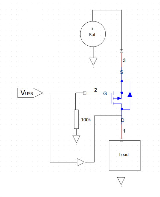
    -Regarding the isolation between USB and battery, I planned to put a P-MOSFET between negative battery terminal and ground, driven by the USB so that battery does no hand any current when usb is present. And also placing a schottky diode between positive battery terminal and Vcc. I am not aware of any drawback on this, but it'd be nice to hear critics. 

    Thanks

  • Hi Mario,

    To increase the life time of the coin cell as much as possible I would recommend using the TPS72630 DCDC regulator. This will reduce the TX and RX peak current consumption from the battery. It is no point in having a boost converter because in all practicality the battery will be dead when reaching 2.0 V volt.

    The PMOS will work fine as you suggest. The schottky diode also, but there will of course be a small power loss through it. The diode should not be required though, since the negative battery terminal is disconnected.

    Cheers,
    Fredrik

  • Fredrik, thanks for such quick reply.

    I also had in mind using a TPS63030 to out a regulated 2.7V. I will check the one said. (you mean the TPS62730 right?) Thanks 

    Agree on the small loss, I will look for smallest quiescent current device out there. Still, if you know of any other more convenient way, please suggest.

    Thanks for your help

  • Hi Mario,

    This sounds a little scary to me but perhaps without a schematic I am not able to properly follow how the connections are being done.  For my comments I am assuming that you are shorting all supplies including the USB supply.

    The PMOS between the battery and ground will certainly disconnect the battery when a high voltage (1) is applied but when a low voltage is applied (0) then you will not get a good short to ground.  Consider that that voltage from source to gate must be above a threshold to turn on the transistor.

    I agree that you need the diode.  If you go without the diode then when the battery is disconnected then the supply to the regulator essentially becomes zero and you will be shorting the USB supply to the regulator output.  This probably violates the operating conditions of the regular to have voltage applied to a signal pin when there is no supply.  Also it could have a strange effect of supplying the regulator through ESD protection that would actually cause the regulator to try and turn on and pull the voltage back down to whatever the regulator is set to.

    With the diode drop you may not be able to use the TPS62730 because the final voltage at the 2540 will be 2.1 minus the drop which could be below the required supply.

    Regards,

    GoBK

  • Thanks GoBK for your comments.

    Yes, I am power switching between USB and a non-rechargeable battery. When USB present, battery should not be

    I believed you could drive a MOSFET with no more than 0-5 V. I attach a little sch on the option of switching based on the MOSFET, maybe we're misleading one another. I guess that could work reasonably well if simulated. 

    Fredrik:

    I've checked the TPS62730, I like the features it delivers, however, I don't think I can use it when power comes from USB. The Vin max is 3.9V. Please, let me know what you think about this, or suggest alternative please.

    Many thanks

  • Hi Fredrik,

    If I want to use the TPS62730 to share two inputs (properly switched between USB and battery). As the input in the DCDC is 2-3.9V, I need to lower the VUSB, can I use a simple divider or I must use an LDO?

    Please reply

    Thanks

  • Hi Mario,

    My comments about the PMOS not working was based on your description of putting the PMOS "between negative battery terminal and ground".  I agree your schematic should work with the PMOS on the positive terminal.  However you may have an issue with your diode.  Your supply to the 2540 will be a diode drop below the USB supply so you'll have digital signals that are 3.3V interfacing with the 2540 which is supplied by a supply which is a diode drop below 3.3V.  Technically this is a violation of operating conditions, practically speaking though it will probably work with the potential of some extra leakage depending on how much the diode drop is.

    GoBK

  • GoBK,

    You're right, I made some changes, initially though, it was thought to be short terminal pin. 

    And yes, the diode drop makes me doubt about this arrangement.

    Many thanks

    Mario

  • Mario Hernandez said:
    If I want to use the TPS62730 to share two inputs (properly switched between USB and battery). As the input in the DCDC is 2-3.9V, I need to lower the VUSB, can I use a simple divider or I must use an LDO?

    Hi Mario,

    I would recommend using an LDO. Alternatively you can consider using the TPS62740.

    Cheers,

    Fredrik

  • Thanks again Fredrik!

    Yes, I'll definitely go for an LDO for the USB (I do not "need" efficiency when USB is plugged). The reason under that is that TPS62740 is more expensive than the sum of TPS62730+LDO. Although, I have been skimming the TPS62740 and it's even more efficient than the TPS62730!!

    My application is based on CC2531, powered by battery and it will combine short periods of TX/RX with periods of sleep. For low loads (supposedly the most common situation), the 740 is really superior. However, the bypass mode on the 730 for when battery is about to die seems very convenient. Can you shed some light on this? I mean, is 740 as superior as it seems?

    Many thanks

    Cheers

  • Chatto said:

    Keni,

    As long as the DVDD_USB is maintained in the 2.0V-3.6V, you should be okay with supplying the USB with a supply other than that of the other VDD.

    You can use the DVDD_USB at a lower voltage than VDD.

    Hi Team,

    This thread has been very informative regarding whether or not USB power can be separate from the rest of the CC2540 pin supplies. That said, I want to verify one last corner case not discussed:

    Can DVDD_USB be supplied at a higher voltage than the VDD of all other pins supplied by the battery?

    For example:

    USB Power stepped down and connected to DVDD_USB = 3.3V

    Battery supplied VDD to all other CC2540 VDD pins = 2.5V

    Is this perfectly fine and won't introduce leakage currents?

    Thank you.

  • Hi Ralph,

    Let's discuss the issues.


    With different supplies you worry about ESD protection diodes and cross domain logic signals interfacing.

    For ESD a lot of times you will see supplies tied together on chip through diodes, so a different voltage will cause the diodes to turn on however for this chip it is not done so this is not a concern.

    Cross domain logic signals:

    1) Signals going from the USB pad to the rest of the chip:

    All of the signals from the USB pad interface go into the digital core which is regulated at 1.8V.  You have a higher input signal driving the internal logic gates, but since they are CMOS this situation is fine.  This situation also occurs regardless of whether your supplies are set the same since it deals with the external USB supply compared to the internal regulator.

    2) Signals going from the rest of the chip to the USB pad:

    All of the signals except for one come from the digital core on the internally regulated 1.8V and are level shifted by the USB pad.  Unfortunately there is one logic signal that comes from a different 3V domain.  This is the Enable signal.  When the chip is not in low power mode than the Enable signal will be high.  In this scenario you will have a 2.5V signal driving into a logic gate supplied by 3.3V, it will work but you will leak some current maybe 50-100uA.  During low power modes there is no problem since the enable signal will be 0V.

    If you can deal with that leakage than it's probably fine, but unfortunately no one has done any testing or reliability so I doubt you'll get any definitive responses.

    Regards,

    GoBK