This thread has been locked.

If you have a related question, please click the "Ask a related question" button in the top right corner. The newly created question will be automatically linked to this question.

Current Savings from a TPS62730 not obesrved

Other Parts Discussed in Thread: TPS62730, CC2540

Recently added control on the TPS62730 to my project.  With this I had expected some current reduction during advertising which would allow me to use +4dB for TX and atleast be on par with 0dB without the TPS62730.  However my observation is as follows:

@ TX: 0dB,  No TPS62730,     TX =  29.2mA  which is around what the datasheet specs (+2mA) 

@ TX: +4dB, w/ TPS62730,    TX = 32.8mA which is over +8mA greater than expected.  

I have scoped the board to verify that the TPS62730 is enabled properly and brings the rail down to 2.1V within the expect Advertising window.  Therefore I am concerned as to why I am not seeing any of the expected current savings.  The consequence of this unexpected high current is that the hardware will POR reset much sooner as the battery depletes and IR increases, vastly reducing expected lifetime on the battery.  Is there anything else besides 

HCI_EXT_MapPmIoPortCmd( HCI_EXT_PM_IO_PORT_P1, HCI_EXT_PM_IO_PORT_PIN2 ); 

that must be set to observe the expected current savings?  Anyone else run a similar issue?   Thanks guys.

  • That API should be all that you need (assuming you specify the correct pin). How are you measuring the current? Are you measuring the current going into the CC2540, or the current going into the TPS62730?

  • Thanks for the reply.  

    I am scoping the voltage across a 10R resistor, going into the TPS62730 Voltage Input.   I was testing with my coin cell battery simulator with an "IR" of 30ohms and noticed that the boards under going POR sooner then usual.  I found that the peak currents were causing enough of a Vbatt drop-down to cause POR resets to the board.  Outside of the datasheet values, what could I expect for real world values at +4dB settings while enabling the TPS62730 (I have scoped this to very it is controlled properly).   I need to gauge the expect POR battery conditions.  Thanks for your help.

  • Kevin,

    When you say POR reset, do you mean the STAT output from the TPS62730, an external POR or the device internal POR?

    When disabling the DC/DC you will see a quite large inrush current due to the capacitors on the chip side (DCDC output) being charged from 2.1V to 3.XV.

    This charge is not "lost" however as it is used by the CC device while the DC/DC output discharges from 3.X to 2.1V when enabled again.

    Have you tried measuring simply static current with / without the DCDC to ensure everything wrt hardware is correct, i.e. while the device is simply halted by the debugger or just running a while(1) loop?

    Note you can also reduce the current by reducing the MCU clock frequency and stop the CPU during radio usage with the APIs HCI_EXT_ClkDivOnHaltCmd and HCI_EXT_HaltDuringRfCmd, though this will affect things such as SPI during RF.

    Regards,
    Svend

  • I see the POR when I capture the SLEEPSTA value upon every reset for debug logging.  I will try those HCI calls, (though I thought those two were enabled by default).   Will also double check the hardware as you instructed and report back.  Thanks for the reply.

  • I enabled the Halt MCU command  HCI_EXT_HaltDuringRfCmd during Init, however I did not see much change in current consumption during RF transmissions.  In fact I actually see an increase in current consumption with the TPS62730.


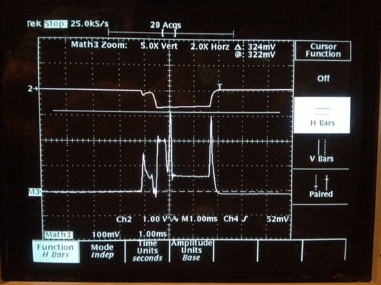
    These are screen captures [ photo since my scope is old ;) ] of +4dB with the TPS62730.  Note the power line showing it is properly dipping to 2.1V during the Connection RF Event. The peak current = 32.4mA


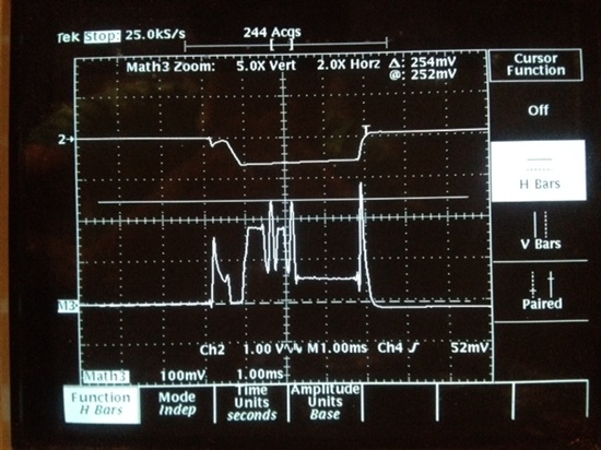
    +0dB with the TPS62730.  The peak current = 25.4mA, (ignoring the current surge after disabling the TPS62730)

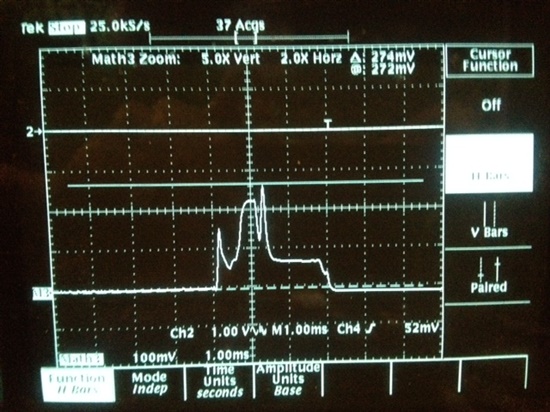
    +4dB without the TPS62730. The peak current = 27.4mA.  Which is odd as this is less than the datasheet values

    Now this was testing on a hardware platform with only 2.2uF of pre LDO capacitance.  Perhaps that is too little to use the TPS62730 effectively, and the resulting voltage switching causes current surges which when factoring in a coin cell battery's IR ( 25-30Ohms after some use ) causes voltage drops with result in PORs?   Please advise, thanks?

  • A 2.2uF capacitor on both the TPS input and output should be enough. You also have a 2.2uH inductor on the TPS output I assume? :)

    The HCI_EXT_MapPmIoPortCmd() will simply set up the argument IO to be used as a DCDC control pin by:

    - Disabling analog mode
    - Select it as a GPIO
    - Set it as output
    - Disable interrupts for the pin
    - Store the IO config (port and pin) in the variable dcdcData  (dcdcData = (ioPort << 8) | ioPin;)


    Then this config is used in ll_sleep.c to turn the DC/DC on/off when going out of / into sleep as long as the POWER_SAVING symbol is defined in the compiler preprocessor.

    I think you should be able to dynamically turn it on/off while your code is running as well by directly writing to the port register as long as your code is blocking the stack from running.

    If you need to keep the pin at a certain level for an extended amount of time you can run HCI_EXT_MapPmIoPortCmd with HCI_EXT_PM_IO_PORT_NONE as port argument.

    Could you test the DC/DC functionality standalone by toggling the DCDC pin yourself through IAR's register view and check whether the current goes down when enabling the DCDC.

    If not, there might be something not working in your hardware setup.

    Regards,
    Svend

  • Do you have a pull down resistor on ON/BYP pin of the TPS?

    I assume you are using the CC2540. confirm?

    You claim to have "2.2uF of pre LDO capacitance", but the TPS is a switching regulator. Do you have two voltage regulators on the same board?

    Instead of using HCI_EXT_MapPmIoPortCmd , set the GPIO high and see if the regulating TPS still contributes +5mA when the CC254x is in a low power mode. 

  • Thanks for the reply guys,  

    As you can see from the screen shots, the regulator is operating as expected.  I called it an LDO due to legacy design nomenclature,  but you are correct its a DC-DC regulator.  Yes there is a 2.2uH inductor

    - I do not have a pull down on the control ON/BYP pin, I connect it directly to the CC2540 p1.2 (as in the TPS62730 datasheet).  

    - The TPS62730 is being enabled and disabled as expected (see screen shots). 

    - I made sure to add HCI_EXT_HaltDuringRfCmd( HCI_EXT_HALT_DURING_RF_ENABLE ); 

    - I did not add HCI_EXT_ClkDivOnHaltCmd( HCI_EXT_ENABLE_CLK_DIVIDE_ON_HALT ); as it affects the buzzer tones during fast connection intervals

    I wrote some test code to keep the Regulator on all the time,  I measured a Iq = 35uA which is the operating quiescent current of the regulator.  Still see peaks up to 30~34mA during advertising.   Connection event peaks do tend to be lower, averaging around 24.8mA, but some peaks exceed 28mA.   Is it expected that Advertising current peaks and Connection current peaks differ this much?   

    I'm really trying to gauge/reduce the maximum peak levels while maintaining range.  For example a fairly depleted CR2032 could have 2.8V and an IR of ~30ohms.   At 30mA peaks, the IR will cause a voltage drop of 0.9V causing a POR reset.  Making the battery useless.  However if these peaks are at a max 26mA, the drop is 0.78V, and no POR.  Extending the useful battery life of the product.  Thanks for the help guys.

  • Kevin,

    Could you verify that the current goes down when doing a static test? For example set a break-point right before the DC/DC is turned off somewhere and compare the current level before and after the instruction toggling P1_2.

    The peaks measured this way might fool you a bit depending on how much data is transmitted. If your connection events don't contain any data then the time in TX will be short. Since you have some capacitance on the board, the peak will be smoothed out and the longer you are in TX the closer you are to see the actual max peak.

    ---

    If as you say the battery voltage is dropping down towards the same voltage as the DC/DC output voltage during TX then you should not see any current improvents but rather an increase in current.

    For a DC/DC, the efficiency E is E= Po/Pi (Power out / Power in).

    If the battery voltage Vi is the same as the output voltage Vo then you will have E = I_out /I_in and I_in = I_o / E.
    Since efficiency is always lower than 1 the measured I_in will actually be higher.

    As a lot of coin cells have quite high source resistance killing the DC/DC efficiency you might try to experiment with larger decouple capacitors on both sides of the DC/DC. This should reduce the battery voltage drop and bring the total efficiency a bit higher.

    Regards,
    Svend

  • Thanks for the reply,

    I have verified that I see the expected quiescent current draw of the active DCDC when I pause the chip before P1.2 is toggled low.

    You are correct, the TX peaks will always depend on data load.  But as a designer I have to account for the max peaks in order to assure that over the lifetime of a battery we maximize the time before POR occur as the coin cell battery's IR goes up.  This maximized the available capacity of a the coin cell battery.  This is something that the current consumption excel sheets do not take into account.  But my observations only ~70% of a CR2032 capacity is actually available to the CC2540.  After that point, the IR >= 30 and an initialization TX peak (high data load) could potentially cause a momentary drop-out resulting in POR.  Which is unacceptable user experience.  

  • I fear that the in-rush current you mentioned may be the culprit for the POR resets I am seeing.  The battery level measures to be around 75% when the device can randomly experience resets.  Sometimes the in-rush is up to 45~50mA peaks.  Couple this with the voltage-drop from a coin cell battery's internal resistance and its a recipe for Drop out Resets.   Unfortunately I cannot add capacitors to our existing hardware platform, but will have to note this for future HW updates.  For now I'll have to stop using the LDO after the battery reaches 80%.

  • Hi Kevin,

    Just one question, how is the DCDC working when you experience the drop and POR, on bypass mode?

    Thanks

  • Correct,  after a certain battery % level I keep the DCDC in bypass mode permanently.  It has only marginally helped but I still can't get reliable operation (no POR) with a battery % lower than 60%.   And have gotten zero support from Ti on the issue.   We may have to switch to Nordic if we can't resolve the issue.

  • Hi Kevin,

    The largest inrush currents will probably be seen when you disable the DC/DC as the DC/DC will then go into bypass mode, causing the chip side to be charged from 2.1V to 3V. 

    As previously mentioned there is not much to be done with this issue except adding decoupling capacitors.
    Another option is to keep the DC/DC enabled at all times which gives a penalty in power consumption instead.

    Best regards,

    Svend

  • Adding more capacitance is definitely a potential for hardware fixes.  However I am trying to stem restarts for existing hardware in the field.  The legacy design was done before I started on the project and followed the Ti App note for TPS62730 implementation.

  • Since you followed the TI reference schematics for the TPS, then you have a footprint for a Cbuf on the battery correct? Just increase the cap's value and your battery won't see the rush of current that svendbt mentioned. Coin cells aren't the focus of the TPS docs.

    TI created a separate white paper for coin cells