This thread has been locked.

If you have a related question, please click the "Ask a related question" button in the top right corner. The newly created question will be automatically linked to this question.

Unable to examine peripheral registers using GDB

Other Parts Discussed in Thread: CC3200, SEGGER, CC3200-LAUNCHXL, UNIFLASH, CC3200SDK

Hello,

 I’m trying to debug the CC3200 Blinky example and I don’t seem to be able to examine any of the CC3200 Application MPU’s peripheral registers.

I have built the Blinky example (and driverlib library) using the GNU ARM tools and I am using the GNU debugger (GDB). My target board is connected using a Segger J-Link using SWD. Any attempt to examine the memory-mapped address of a peripheral register results in an error.

 For example, if I try to examine the GPIODATA register for GPIO Port A0 (at address 0x40004000) I see:

 Cannot access memory at address 0x40004000

 I have no problem reading addresses in SRAM or ROM, or the CPU core registers.

 I have tried using the GDB command set mem inaccessible-by-default off but it did not solve the problem.

I can step through the Blinky software running on the target but it is not blinking the LEDs (two of them are always on, the red one always off). It’s going through all the motions, just not actually accomplishing anything.

 Can anyone suggest reasons why I cannot examine the peripheral register locations?

 Thank you.

  • Hi Steve,

    We are able to read memory-mapped address of peripherals register. We are using 

    (gdb) x 0x40004000

    0x40004000:        0x00000000

    To debug your issue please provide following information:

    1. is it customize board?

    2. Is it standard sdk application or you modified the code and linker file?

    3. Device and SDK version.

    Regards,

    Aashish

  • Hi Aashish, thank you for replying.

    I’m glad to see you are able to examine those registers – it gives me hope :)

     To answer you questions,

    1. Is it customize board?

    It is a CC3200 LaunchPad board (CC3200-LAUNCHXL).

    2. Is it standard sdk application or you modified the code and linker file?

    The source files and linker file are straight from the SDK examples with some very minor changes:

    I added the following sections to ‘main.c’ to accommodate the gcc toolchain (ccs and ewarm sections were already present)

    #if defined(gcc)

    extern void (* const g_pfnVectors[])(void);

    #endif


    #if defined(gcc)

       MAP_IntVTableBaseSet((unsigned long)&g_pfnVectors[0]);

    #endif


    I modified the linker file ‘blinky.ld’ to reduce the size of the SRAM region so that it matches the XCC3200HZ device.

       /*SRAM (rwx) : ORIGIN = 0x20004000, LENGTH = 0x3C000 */

       SRAM (rwx) : ORIGIN = 0x20004000, LENGTH = 0x2C000

     3. Device and SDK version.

    XCC3200HZ device variant.

    SimpleLink SDK version 1.0.0 with service pack 1.0.0.1.2 installed on the device.

    I am actually using emIDE for my development environment, so when debugging I use the IDE to send specific commands to the GDB debugger and/or the GDB server.

    Thanks!

    Steve

  • Hi Steve,

    We tested on same device CC3200-LAUNCHXL (XCC3200HZ)  with SDK 1.0.0's example, service pack 1.0.0.1.2 and without making any changes in main.c and blinky.ld on Linux environment without any issue. May we know why did you make changes? Also why are you using JLINK debugger as board already have USB based FTDI debugger. You can find more details for GCC environment in "docs/CC3200-Programmers_Guide.pdf"  section 5.3.3 "Development Environment – Open Source" 

    Regards,

    Aashish

  • Hi Aashish,

    I made those changes to the ‘main.c’ to follow the same pattern as for the CCS and EWARM toolchains. The change should have no effect in this program because it appears that calling MAP_IntVTableBaseSet() is only required if using the API to call MAP_Integister() (which is never done in the Blinky example). Modifications to blinky.ld were made after I couldn’t get the code to work so I wanted to make sure that the linker was staying within the SRAM area supported by my device.

    I’m using the J-Link debugger for a couple of reasons:

    1)      It is the only one supported by the (free, and generally very good ) IDE that I am using (emIDE).

    2)      In the future I would like to make my own custom board and not have to implement the debugger that is on the Launchpad.

    I have recently discovered that if I use the Uniflash tool to install my Blinky.bin image into the SFLASH device it still does not work (judging by the LEDs not blinking). However, if I load the Blinky.bin image that comes with the SDK it works perfectly. So that leads me to believe that there is something wrong with the driverlib library and/or the blinky example that I have built.

    Thank you for referring me to the CC3200-Programmers_Guide.pdf and the section on open-source development. I have actually studied that and also examined the files in C:\ti\CC3200SDK_1.0.0\cc3200-sdk\tools\gcc_scripts as well as the makefile for the gcc blinky example to make sure that I was using the correct compiler and linker options for gcc.

    To return to my problem of not being able to read the values in peripheral registers, I added some code to my program to see if I could read the registers from there and found I cannot.

    unsigned long regs[10] = {0x00000000};

    BoardInit();

    regs[0] = *(unsigned long *)(0x40005000 + 0x000);

    regs[1] = *(unsigned long *)(0x40005000 + 0x400);

    The program either gets stuck at an assembly instruction that is trying to load the register value into a cpu register, or it occasionally winds up trapped in the FaultISR handler.

    Even stranger is that for a small window of time I was actually able to read the registers associated with GPIO Port A1 (at address 0x40005000) using both GDB commands and my test code that loads them into regs[]. However it only worked with GPIO Port A1. Any attempt to read registers for any of the other three GPIO ports would not succeed.

    I’m pretty stumped right now as to why this will not work. There are so many different things not working that I don’t know what is a cause and what is an effect.

    Steve

  • Hi Steve,

    Please share modified project with us. Also try modified code as mentioned in CC3200-Programmers_Guide.pdf for opensource compiler with on board FTDI debugger (Don't use emIDE and jlink for this test).

    Regards,

    Aashish

  • Hi Steve,

    By default the modules are clock gated and are not accessible. Accessing a module when in clock gated state will generate a bus fault.

    To access any module you first need to enable it by invoking MAP_PRCMPeripheralClkEnable() with appropriate parameters.

    Referring to blinky example, the GPIO module is enabled in PinMuxConfig() function. From your above code looks like you are trying to read from GPIO before it is enabled.

    Can you please push this code below the PinMuxConfig() function call and try again ? Let me know the result.

    Regarding, compiling blinky on your setup, were you able to make this work ? If not, two things you need to make sure

    1. The code is compiled for SRAM range starting at 0x20004000.
    2. The vector table is placed at 0x20004000.

    Both these things you can check by generating the map file.

    Thanks and Regards,
    Praveen
  • Hi Praveen,

    Thank you for your help. I moved my attempts to read GPIO Port A1 registers to after the call to PinMuxConfig() and indeed, once the clock has been enabled on the GPIOA peripheral I can read the registers both using my debugger and through my program. That is one mystery solved at least!

     I even implemented the following test:

    bIsGPIOReadyBefore = PRCMPeripheralStatusGet(PRCM_GPIOA1);

    PinMuxConfig();

    bIsGPIOReadyAfter = PRCMPeripheralStatusGet(PRCM_GPIOA1);


    As expected, the call to PRCMPeripheralStatusGet() returns false prior to calling PinMuxConfig() and returns true afterwards.

    However, while my program does appear to run the Blinky example, it will not change the state of the LEDs. With regards to the location of the vector table, the following excerpt from my map file shows the following:

     .text           0x20004000     0x2a60

                   0x20004000               _text = .

    *(.intvecs)

    .intvecs       0x20004000     0x400 obj\Debug\Setup\startup_gcc.o

                   0x20004000               g_pfnVectors

    *(.text*)

    .text.ResetISR

                   0x20004400       0x6c obj\Debug\Setup\startup_gcc.o

                   0x20004400              ResetISR

    .text.NmiSR   0x2000446c       0x8 obj\Debug\Setup\startup_gcc.o

    .text.FaultISR

                   0x20004474       0x8 obj\Debug\Setup\startup_gcc.o

     And if I use the debugger (GDB) to examine the memory I see everything is correct:

     > x /3 0x20004000

    0x20004000 <g_pfnVectors>:    0x20007a80     0x20004401     0x2000446d


    What I don’t understand is that when I start my program up and it is sitting at a breakpoint at the beginning of main(), the Green and Yellow LEDs on the Launchpad board are on. I would have thought that the output pins would be in a high-Z state at that point. So what I did was step through the code until after the call to PinMuxConfig() and then took a closer look at the GPIODATA register for the GPIO Port A1 peripheral.

     Examining the data register:

     > x 0x400053fc

    0x400053fc:    0x0000000c

    That is consistent with the Green and Yellow LEDs being on (since bits 1, 2 and 3 in GPIODATA control the Red, Yellow and Green LEDs repectively).

    I then used to the debugger to write to the GPIODATA register and got these results:

     set {unsigned long}0x400053fc = 0x00000000

     The green and yellow LEDs both turn off.

     set {unsigned long}0x400053fc = 0x0000000e

     The Red, Yellow and Green LEDs all turn on.

     Yet calls to the MAP_GPIOPinWrite() in my Blinky example do nothing.


    Thanks again for your input,


    Steve

  • Hi Steve,

    Regarding Yellow and Green LEDs on by default, these lines are used as I2C lines on LP thus have external pull-up. If you remove the jumpers J2 and J3, you will see these LEDs are off by default.

    Regarding MAP_GPIOPinWrite(), can you please re-compile the Driverlib on your setup and try to step into the function to see whats going wrong ?

    Thanks and Regards,
    Praveen
  • Hi Praveen,

    Thanks for pointing out those pull-ups that I should have noticed ;)

     I’m not sure if this is what you were suggesting but I rebuilt the driverlib library so that it does not use the ROM instance of GPIOPinWrite.

     In rom_patch.h I added the line

     #undef      ROM_GPIOPinWrite

     After rebuilding the library and re-linking my Blinky example everything works great, the LEDs are blinking away as they should.

    I then stepped through the assembly instructions that preceded the call to GPIOPinWrite procedure and examined how the arguments were being passed using the CPU registers. This is what I can see happening for both RAM and ROM versions of GPIOPinWrite:

     ROM API for GPIOPinWrite

    void GPIOPinWrite(unsigned long ulPort, unsigned char ucPins, unsigned char ucVal)

    State of the CPU registers immediately before the branch instruction:

    r0 = 0x40005000                (ulPort)

    r1 = 0x08                              (ucPins)

    r2 = 0x00                              (ucVal)

    The instruction that branches to the GPIOPinWrite procedure is:

    bl            0x20004fc4 <GPIOPinWrite>


    ROM API for GPIOPinWrite

     State of the CPU registers immediately before the branch instruction:

    r0 = 0x40005000                (ulPort)

    r1 = 0x08                              (ucPins)

    r2 = 0x00                              (ucVal)

    r3 = 0x7503                         GPIOPinWrite

     The instruction that branches to the GPIOPinWrite procedure is:

    blx          r3


    As far as I can see, everything looks correct in both cases, yet the call to GPIOPinWrite in ROM does not work. I looked at rom.h and rom_map.h in driverlib and using the debugger and the ROM_API TABLE and ROM_GPIOTABLE offsets I determined that GPIOPinWrite should be located at address 0x7503 in ROM.

    Is there perhaps some strange calling convention that the ROM API is using?

    Thanks again,

     Steve

  • Hi Steve,

    Let me check and get back to you.

    Thanks and Regards,
    Praveen
  • Hi Steve,

    Can you please post here the version printed on the device. It would be something like this "CC3200??"

    Thanks and Regards,

    Praveen

  • Hi Praveen,
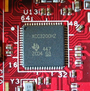
    It is XCC3200HZ. Let me know if you need any of the other information printed on the package.
    Thanks,
    Steve
  • Hi Steve,

    It is a pre-production part. The ROM APIs are only supported on production part CC3200R1.


    Thanks and Regards,

    Praveen

  • Hi Praveen,

    I suspected that it might be a pre-production part.  However I am wary of the idea that it doesn't support the ROM APIs for a couple of reasons.

    For one thing, earlier in this thread Aashish indicated that he was able to get the blinky example to run, unmodified, on exactly the same board and XCC3200HZ device as I am using.

    Also, I took the blinky.bin file that comes with the SDK (C:\ti\CC3200SDK_1.0.0\cc3200-sdk\example\blinky\gcc\exe\blinky.bin) and used Uniflash to install it on my board, and it runs just fine.  I seems strange to me that the pre-built binary of the example would have used a build of the driverlib library that was not using the ROM APIs.

    Is there any way to find that out for sure?

    Thanks,

    Steve

  • Hi Praveen,

    Ok, I did some more digging and I think that you are right about the ROM APIs not being supported on the pre-production XCC3200HZ device.  Actually it would probably be more accurate to say that there appear to be a different set of ROM APIs on the pre-production device.

    I used my debugger to examine the instructions that were being executed from ROM when I called GPIOPinWrite() and disassembled them to the following:

    .data:0x00007502   6080f500    add.w r0, r0, #1024 ; 0x400

    .data:0x00007506       6802    ldr r2, [r0, #0]

    .data:0x00007508       4311    orrs r1, r2

    .data:0x0000750a       6001    str r1, [r0, #0]

    .data:0x0000750c       4770    bx lr

    It appears that whatever API is located at 0x7502 is actually used to set the direction of a pattern of GPIO port pins to be outputs. My guess is that it takes 2 arguments, the GPIO port base address (passed in r0) and a pin mask (passed in r1). It then ORs the mask with the port’s GPIODIR register (at offset 0x400).

    The closest thing to that in the peripheral API is the function GPIODirModeSet(), but it takes 3 arguments. So I have to conclude that my device’s ROM contains an undocumented prototype API.

    Well, at least now I know!  I'll have to see if I can get a newer CC3200-LAUNCHXL launchpad board that has a production part on it.

    Thanks again for all your help.


    Steve

  • Hi Steve,

      Would you send either a description, or a picture, of the Revision information on the CC3200 LaunchPad you are having difficulties with, please.  Also, there are revision notes on the CC3200 WIKi, as well as a lot of other information, not sure if you have explored this?: http://processors.wiki.ti.com/index.php/CC31xx_&_CC32xx . 

      (FYI, I support Andrew and his team, even though I am located in Dallas, so that is what prompted me to contact you.)

    ~Leonard


  • Hi Leonard,

    Thanks for the link to the Wiki - I had looked there for a few things but hadn't yet explored it thoroughly.  I did just now find the table of hardware revisions showing my device listed as pre-production.  Below is a photo I took showing the CC3200 part on my LaunchPad board.

    Steve

  • Hi Steve,

      We can either send you a CC3200 for replacement on the EVM, if you have the ability to rework this pcb.  Or we will have to arrange for an exchange of the EVM.

    Let me know your preference.

    ~Leonard

  • Hi Leonard,

    Technically I do have the tools to re-work the PCB but realistically I don't see that going well - would probably go from a' sort-of' working board to a 'not-working' board ;) Therefore the option for a new LaunchPad board would be my preference.

    Thank you,
        
    Steve