This thread has been locked.

If you have a related question, please click the "Ask a related question" button in the top right corner. The newly created question will be automatically linked to this question.

TRF7970A: TRF7970A internal regulators

Part Number: TRF7970A

hi,

i have a question concerning the 3 internal regulators of the TRF7970 (VDD_X, VDD_RF, VDD_PA).

in the datasheet it is noted that the 3 regulators turn on after EN pin goes high. (EN2 pin is on ground; VIN=3.3V)

now i noticed in my circuit that only VDD_X and VDD_A turn of after EN -> high but VDD_RF turns on  immediately after there is voltage supplied on the VIN pin.


è Do you know if this is normal or what the problem could be?

è Because I want that all 3 regulators turn on after EN -> high


thanks a lot

regards

chris

  • where in the data sheet are you reading that?
    Anyway - VDD_X is the only regulator that you should care about as the others are for use by the IC internally, you cannot connect anything to them which requires additional current. Only VDD_X is allowed for your use.

    look @ 6.3.3 on page 19 == > www.ti.com/.../trf7970a.pdf
  • thanks for the information!

    i found this on page 19 of the datasheet:

    "The main reader enable signal is pin EN. When EN is set high, all of the
    reader regulators are enabled........"

    ->i understood that i can only use VDD_X for external supply
    -> i don't use VDD_A and VDD_RF for external supply

    but i dont't understand why VDD_RF is enabled before EN goes high? Because in the datasheet it is noted that all regulators are enabled after EN -> high
    and in my case -> this is only true for VDD_A and VDD_X?

    thanks!
    chris
  • would you share your schematic, please?
  • yes of course but i don't know how to post a schematic in the forum?
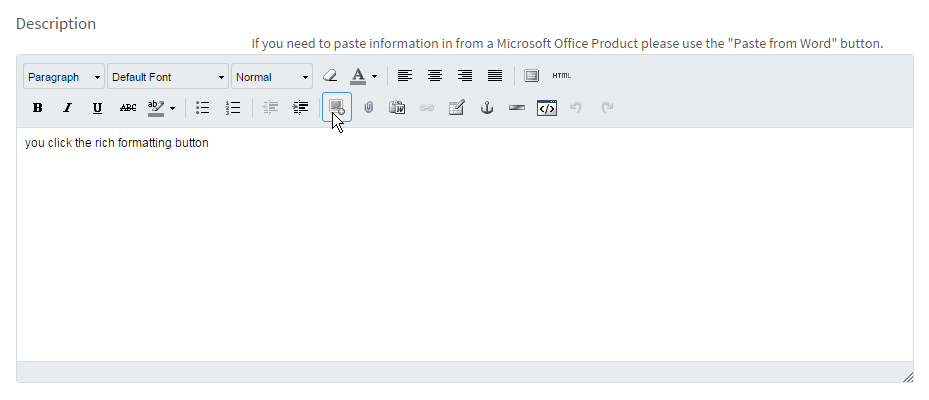
  • you click the rich formatting button

    then click insert media, browse, choose your file, then insert.

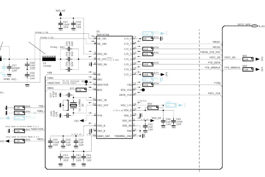
  • in my case R83 is not mounted and R84 is mounted!
  • understood - so you don't use VDD_X at all here -

    here is what i see - and the schematic could be redrawn a bit to make it easier to read, but its yours - so your call :)

    MOD pin is pulled high to 3.3VDC, should be pulled low through 1k and the pin connected to MCU if you in fact want to use DM0 at some point.

    ASK/OOK pin also is recommended to have 1k pulldown as well - might work with 10k but if memory serves, that should be a harder pull down

    the resistors on the SPI lines are not necessary - R74, R75, R76, R79 and the R71 on the MOD pin - not sure why you put those in

    Vin requires bulk and high speed bypass caps - in fact, there should be five pairs of these in your design (on VDD_X, BG, VDD_PA/VDD_RF, VDD_A and VIN)

    i see you have most of that covered, but nothing shown for Vin and only 1uF on VDD_X

    your drawing of the lines out - particularly the handling of I/O_3 and 5 is not clear. normally those are left open for SPI w/SS and you could use VDD_X to keep the I/O rails correct simply.

    i cannot see the entire matching network - please check with what i attached here below.  

    attached is the reference schematic and layout for SPI w/SS

    TRF79x0ATB_SCH_C.pdf

    TRF7970ATB_PCB_D.pdf

    additionally, since you are using split rail (which can be done) - here is a good app note about that

  • thanks for the information!

    one more question:

    -> i don't want to use the DM0 mode in the future -> so can i put mod pin to 3V3 like in my circuit without getting any problems for normal ISO15693 operations using SPI with SS?
    (because i dont want a redesign :-) )

    -> i didn't found the information in the datasheet that i schould use 1k to GND for the mode pin -> can you tell me the page ?

    thanks a lot
    chris
  • correct
    the pull down resistor values for MOD and ASK/OOK are in each of our reference designs. (one of which i gave here directly, they are all online, too)