This thread has been locked.

If you have a related question, please click the "Ask a related question" button in the top right corner. The newly created question will be automatically linked to this question.

TRF7960A: Unexpected switch of SYS_CLK from 6.78 MHz to 60 KHz.

Part Number: TRF7960A
Other Parts Discussed in Thread: MSP-FET, TRF7960

Hello,

We implemented an RFID reader with a TRF7960A to read and write ISO15693 tags.

Sometimes, the reader doesn't reply to the MCU (MSP430) during Inventory request. After investigations, we found that SYS_CLK from the front-end has switched from 6.78 MHz to 60 KHz.

This state is documented in the datasheet as a "sleep mode", given by EN = 0 and EN2 = 1:

But, in our design, the EN2 pin is connected to VIN and EN is set to 1 by the MCU during the boot.

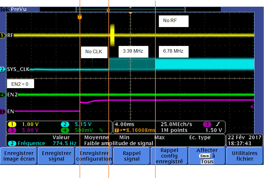
Here is a screenshot to describe what happen : Yellow = Antenna signal. Blue = SYS_CLK. Pink = EN.

You can see that SYS_CLK is 60 KHz before EN = 0. (EN go to 0 after, because we initialize an interruption to reboot the MCU when the clk is missing)

Is it possible to go to this state for another reason, like oscillator unstable for instance?

Is someone meet this kind of issue ? Is it a known problem by TI?

Thanks for your attention.

Pat.

  • Hello Patrick,

    This is not a known problem nor is it one we have seen before.

    Is your system running at 5V? Have you checked the voltage level on EN2 when this issue occurs? I know it's connected to VIN but it would still be good to verify the voltage levels. I don't suspect it will be an issue but would like to validate that it is correct for starters.

    Is the TRF7960A configured for the right voltage setting in Register 0x00?

    The unstable oscillator idea doesn't seem likely, but it can be checked by reading the RSSI Levels and Oscillator Status Register (0x0F) and checking Bit 6.

    Can you share your schematics for this application with us?
  • Hello Ralph,

    Thank you for your quick answer.

    The TRF7960A is running at 5V and the MSP430 at 3.3V, provided by VDD_X from the front-end. Here is the schematics: (EN2 is connected to VIN not to GND, there are pull-down resistors on EN and EN2).

    Yes, I checked the voltage on EN and EN2, both are set to 1 (3.3v). Actually, according to the datasheet, when EN = 1, the state of EN2 isn't important, isn't it ?

    The content of Chip Status Control Register is 0x01, so for 5v operation.

    It seems to me that the problem is internal of the TRF...

    Additional information : This problem occurs only when there is a collision in a special RF environment: 2 tags seen by one antenna, difficult to discriminate.

    Let me know what you think about the tests I can run to go forward to this issue.

    Pat.

  • Hi,

    here is a table to summarize the behavior of our reader, after power-up, regarding the pins EN and EN2.

    In red, the states not compatible with the datasheet:

    EN

    EN2

    VDD_X

    SYS_CLK

    RF_OUT

    0

    0

    2,7v

    OFF

    OFF

    0

    3,3v

    3,3v

    60 KHz

    OFF

    3,3v

    0

    3,3v

    6,78 MHz (0x21 @0x09)

    OFF (0x01 @ 0x00)

    3,3v

    3,3v

    3,3v

    6,78 MHz (0x21 @0x09)

    ON (0x01 @ 0x00)

    Do you have some explanations on that ?

    More details on the behavior according to EN2 at power-up: It seems to me not understandable !

  • Hello Patrick,

    Regarding the following:

    EN

    EN2

    VDD_X

    SYS_CLK

    RF_OUT

    0

    0

    2,7v

    OFF

    OFF

    0

    3,3v

    3,3v

    60 KHz

    OFF

    3,3v

    0

    3,3v

    6,78 MHz (0x21 @0x09)

    OFF (0x01 @ 0x00)

    3,3v

    3,3v

    3,3v

    6,78 MHz (0x21 @0x09)

    ON (0x01 @ 0x00)

    For VDD_X:

    I have tested this on TI hardware and it seems that VDD_X stays at 2.7-2.8V with EN and EN2 off. We will need to do further testing to verify this is not being back powered by anything. This may result in a datasheet change if it is verified that is the behavior.

    For RF_OUT:

    I have tried to re-create this, but I have not had any success. To be certain, the RF_OUT pin you are checking is the "TX_OUT" pin?

    Are you pulling MOD and ASK/OOK down with your MCU?

    Have you read out any registers beforehand to verify 0x00 is set to 0x01? If so, are you using SPI or Parallel mode?

    Are you probing the TX_OUT line before or after the PE42440 switch?

  • Hi Ralph,

    For VDD_X, give me an update when you confirm this point.

    For RF_OUT:

    • The MOD and ASK/OOK pins are set to 0 by the MCU.
    • Here is a screenshot to show the link between the EN2 state (0-3.3v) and the TX_OUT pin : It seems that it works as a AND gate.

    The behavior is normal when I put EN2 to 5v : It's strange because VDD_IO is connected to VDD_X = 3.3v.
    I assume that the EN2 pin must be connected to VIN, even if VDD_IO = 3.3 v. Does it mean that EN and EN2 are not linked both to VDD_IO ?

    Abstract of datasheet:

    A direct connection from EN2 to VIN to ensure the availability of the regulated supply VDD_X and an
    auxiliary clock signal (60 kHz, SYS_CLK) for an external MCU.

    •     I have the possibility to write registers in the front-end at anytime : No change on TX_OUT pin when I write 0x01 @ 0x00. To be sure, I set half power by writing 0x11 @ 0x00 and the signal amplitude decreases.


    These gaps versus the datasheet are very strange but my first concern is the switching to 60 KHz. Do you have some new ideas on this ?

    Best regard,

    Pat.

  • Hello Pat,

    Sorry for the delay in response but I had to run a number of tests first.

    First, to address the switching to 60kHz which you have reported, I have tried to re-create this issue with the TRF7960A and have not had any success in doing so.

    I used multiple ISO15693 tags to create collision errors but do not see any change in SYS_CLK while EN2 is high or low.

    Furthermore, I could not re-create the behavior with the TX_OUT and EN2 acting like an 'AND' gate either.

    Have you tried using a second board or swapping the TRF7960A on your board at all? I would like to know if the issue is isolated to that single TRF7960A or if it occurs with multiple TRF7960A's either on the same board or across multiple boards...

    For VDD_X, we were able to confirm that the voltage output is 0V for EN = 0 and EN2 = 0, when the VDD_X node is isolated. However for the TRF79xxAEVM designs (which your schematic seems based on), it is not trivial to isolate this node, so I would not worry about the VDD_X voltage for your case. If you really do want to measure to see the 0V, also keep in mind you may need to unload the stored voltages on the capacitance of the VDD_X line as well.
  • Hi Patrick,

    I just realized something very crucial, sorry for that catching this earlier.

    You said you have the EN2 line tied to VIN which is 5V correct? EN2 should not be greater than VDD_IO in voltage, and if you have VDD_IO tied to VDD_X then you would around 3-3.5V on that. EN2 can't be connected to 5V in that situation.

    If you ran the TRF7960A for extended periods of time with EN2 connected to 5V, then it is possible you may have damaged the device.

    I noticed that your design is based of the TRF7960AEVM, and reviewed that schematic and can see where the schematic may have mislead you on this. We are going to review the schematic further and make some note or modification to it in order to specify not to route EN2 to VIN for 5V systems unless VDD_IO will be set to 5V as well.

    Please swap the TRF7960A on your board and connect EN2 to a 3.3V rail, and then see if you have any further issues... if not, this may be the source of the problem.

  • Ok Ralph,

    Thank you for your comments.

    I'm going to test with another board to check if the behavior is the same.

    I'll give you the results.

    Regards,

  • Hi Ralph,

    I tested another board with the same results:

    • When EN2 is connected to VDD_IO, RF is always turned ON.
    • Sometimes, when collisions occur, the SYS_CLK switches to 60 KHz.
    • When EN = EN2 = 0, VDD_X = 2.7v.

    You are right about the source of our schematic, it comes from the TRF7960AEVM.

    Could you explain your comment :"However for the TRF79xxAEVM designs (which your schematic seems based on), it is not trivial to isolate this node, so I would not worry about the VDD_X voltage for your case."

    In our case, all the capacitors are discharged at power-up, and we have immediately the 2.7v voltage. However, it seems to me that in this case described in the datasheet, EN = EN2 = 0, VDD_X = 0 and the reader should not startup, isn't it ?

  • Hello Patrick,

    The VDD_X line is connected back to the MSP-FET emulator circuit through R1 and R5. So the voltage you are seeing isn't coming from the TRF but off of this circuit. If VDD_X is isolated from this node and then the caps are discharged, the VDD_X voltage is at 0V with EN=EN=0. However, making these changes messes with the MSP circuitry and prevents the MSP430 from operating correctly thus also rendering the TRF7960A not able to operate as it is dependent on the MSP430. Hence why I said it is not trivial to isolate these nodes.
  • Hello Ralph,

    It seems to me that there is a misunderstanding: There isn't an emulator connected during my test, so the only source for VDD_X is the TRF.

    And I confirm that, in this case, VDD_X=2.7v at power up when EN=EN2=0.

    Here is the voltage sequencing when EN2 = 0 via a pull-down, WITHOUT emulator connected. You can see that VDD_X is set to 2.7v before EN = 1.

    Could you confirm that you don't have this behavior with the TRF7960AEVM and without emulator ?

  • Hello Patrick,

    I am aware the emulator wouldn't be connected. On the TRF7960AEVM without isolating the VDD_X node I saw the same voltage as you do on the VDD_X. However, when it comes to testing these elements regarding the device specifications, we have a TRF79xx Test Board that is used to help isolate the parts of the device under test from outside influences. Using this board, the VDD_X behavior was confirmed by myself and our product test team both to match the datasheet.
  • Hello Ralph,

    I watched deeper our boards and I have an information : We use TRF7960 and not TRF7960A.

    From my knowledge, the main difference between both is focused on ISO14443 communication.

    Is there additional difference that could explain my behavior ?

    Regards,

    Pat

  • Hello Patrick,

    My understanding is the same, but I will go ahead and run the TRF7960 through the same batch of tests on my end and see if I can reproduce any of the reported behaviors with that device as well. I should be able to finish the testing today but if not then certainly by Monday.

  • Hello Patrick,

    I ran through the tests once again and the results matched what I saw with the TRF7960A.

    Regarding the issue with the SYS_CLK switching to 60kHz, you mentioned that it occurs when tags collide due to more than 1 being placed on the same antenna. Is there more detail you can provide about this so I can try and replicate that exact condition? I used 2 ISO15693 tags and didn't see any changes in SYS_CLK. Is this something which happens frequently or sporadically? Which tag technology causes it (maybe not ISO15693?) and approximate what size are those tags?

    The more details you can provide to help me replicate that specific situation the better I can try and match my setup to your own.
  • Hello Ralph,

    I agree, it will be better if I can explain exactly the context of the issue.

    I prepare this for next week.

    Regards,

  • Hello, Ralph,

    I'm going to try to describe our application and the context.

    • Tags used : ISO15693.
    • Size of the tag antenna = 38 x 22.5 mm.
    • RFID chip = NXP SLI-S

    We have 3 antennas to address 3 different tags, thru a RF switch.. Here is the way to discriminate them:

    • We begin with an Inventory request command from our CPU to the reader. Sometimes, one antenna sees two tags.
    • After that, the reader has to read one block of memory of each tag seen, in order to provide the UID of the expected tag to the CPU. (Filtering by content)
    • The HF is stopped after each command.

    Normal behavior, with 2 tags seen and no discrimination problem: (General view on the first screenshot and the detail on the second).

    In some cases, when two tags are seen in a "conflictual position", we have collision and the following behavior.

    Abnormal behavior, with 2 tags seen and collisions:


    And after a moment in this configuration, SYS_CLK switches.

    Abnormal behavior, with 2 tags seen and collisions, SYS_CLK swith :


    Let me know if this is clear and helpful.

  • have you already shared your schematic? might be good to review it (or again) if you have not - you can see noise on the EN and EN2 lines - not saying that this is the root cause, but its clear you have something going on in that last capture. (that is clock off, not switching to another frequency)

    also, what is the Q and impedance of your reader antennas (@13.56MHz)? and how close are they to one another?
  • Hello Josh,

    I've already shared the schematic. It could be a good thing to review the full exchange on this topic, a lot of information have been given, especially on the EN/EN2 state regarding the SYS_CLK switching.

    Thanks in advance.

  • Additional information about Antennas :

    Antenna L1


    Antenna L2:


    Antenna L3:


    Mechanical drawing of the PCB: (mm)


  • Hello Patrick,

    When you say 'In some cases, when two tags are seen in a "conflictual position", we have collision and the following behavior.' - does this mean if you look at the TRF7960 SPI lines, you receive an IRQ of 0x02 to indicate a collision error has occurred per the IRQ status register table on Page 31 of the datasheet? What the IRQ Status register reports in this "conflictual position" is key for my understanding of what possible states the TRF7960 could be in to try and recreate those states on my end.