This thread has been locked.

If you have a related question, please click the "Ask a related question" button in the top right corner. The newly created question will be automatically linked to this question.

TRF7960A: Two questions about TRF7960A external power amplifier

Part Number: TRF7960A
Other Parts Discussed in Thread: TRF7970A

Hello,

Here are two questions,

1. According to your TRF7970A external power amplifier document, I may simplify this design for 1W RF power output if only using one receiving signal RX_IN1 and 100% modulation transmitting, optional RX filter and external modulation control can be not needed, is it correct?

2. When transmitting TP05 signal Vpp is 20V, RX_IN1 input resistance in datasheet is 10kohm, Vpp value of input signal is about 10V from calculation(voltage divider resistance 3.9kohm), so it exceeds Maximum RF input voltage at RX_IN1(3.5V). can the TRF7970A chip be damaged?

Thanks

Brian

  • Hello Brian,

    If you are referring to the power amplifier document "appnote_trf796x_pwramp_4w.pdf" from sloc132, we have removed this design from the web and do not support it any more.

  • Hi Ralph,

    glad to see you again, this work was suspended for some time due to some other things. I am referring your updated design Eddie attached last time.

    e2e.ti.com/.../1896894

    Thanks

    Best Regards

    Brian

  • Hi Brian,

    Ah I see. I am not knowledgeable about that design at all. It isn't an officially released one either, but I'll go ahead and ping a couple engineers who would be able to answer some questions about it and bring this post to their attention to see if they can provide some feedback.
  • Brian - 

    For question #1:

    the mod control can be set for 100% ASK and the switch part of the circuit is not really needed at that point, since the TRF79xxA will do it for you normally, because you set up the part to have the amp attached via register writes to 0x09 and 0x0B, you do still need the variable voltage divider to adjust your depth correctly, based on the rail, then you can move to fixed value

    for the RX portion of the question, you can connect one or both of them, your choice. The dual RX'ers are handy if you know you have read holes, if you don't then you only need the one. 

    For question #2:

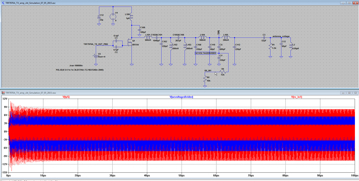
    the 3.9kOhm resistor in that design is for dampening the input to the RXIN_1 pin. Simulation shows with 9VDC, i had to move it to 12k

    see here the simulation results which match. Note this is with 9VDC on the rail of the FET,  which is the highest i ever ran it at. Most of the applications were for meeting EMVCo, so 6.1 to 6.3VDC sufficed in those cases, to create the correct operating volume.

  • Thank Ralph and Josh very much.

    1. If I use this simulation circuit you attached, is it enough that I configure the registers like this way?
    i. For Modulator and SYS_CLK Control Register (0x09)
    B6 =0 not use external modulation control
    B2B1B0 =001 modulation OOK 100%
    ii. For Regulator and I/O Control Register(0x0B)
    B6 =1 support external power amplifier

    Sorry,I did not understand what you said "still need the variable voltage divider to adjust your depth correctly".
    Could you explain more about this?

    2. It is clear for Q2

    3. one more question
    "The complete filter is matched to Zin = (45+j7) input and Zout = (57−j3) output impedance at 13.56MHz" is described in this document, I analyzed impedance transformation from TP03 to TP06 using smith chart tool,impedance at TP06 is 42-j31,it is big different from 57-j3, is there any problem on my analysis?
    for class E power amplifier,C1(150pf)/C2(1040pf)/L2(560nH) can be adjusted to achieve the best efficiency and signal shape according to figure 8 in the document, the value of C1 is different from the one of C100 (100pf) given in your simulation circuit, which value should I use?

    Thanks
    Best Regards
    Brian

  • Hi Ralph and Josh,

    I have done one hardware board according to your circuit, It will be available very soon. Hope that I can have a good understanding from software and hardware point before debugging. Could you have time to support my questions?

    Thanks.

    Best Regards

    Brian 

  • Hi Brian,

    From a hardware side, we don't officially offer support for the power amplifier design, again, not an officially released design. You are free to ask questions and if Josh or any others have the spare time they can chime in but we cannot promise support for that.

    Software wise I can try and help out with, especially if you use TI firmware.
  • Hi Ralph,

    Ok, thank you for letting me know this, I worry that the questions are missed easily when waiting for a long time, can I send the questions to Josh's or any other's email? 

    Thank you for your support, it works well after porting your firmware on the TRF79XX. It is more robust than the old one I used ever, do you have newer version now?

    Thanks

    Best Regards

    Brian

  • Brian - 

    i also monitor this forum too - but i moved to another product group about a year ago - so i don't have alot of extra time, but i will try to have a look at your other post in detail and come back to you as soon as i can.

  • Hi Josh,

    I am glad that I can get your continuing support and thank you for your valuable time.

    I have gotten this board, it is a little different from your circuit.

    L101/L104         538nH (replacing 560nH in your circuit)

    L105                  422nH (replacing 390nH  in your circuit)

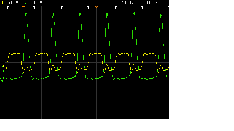
    Vgs(channel 1: Vpp=7V ) and Vds(channel 2:Vpp=47.8V) waveform is shown, less duty ratio and high peak-peak value comparing to fig 9 in the document

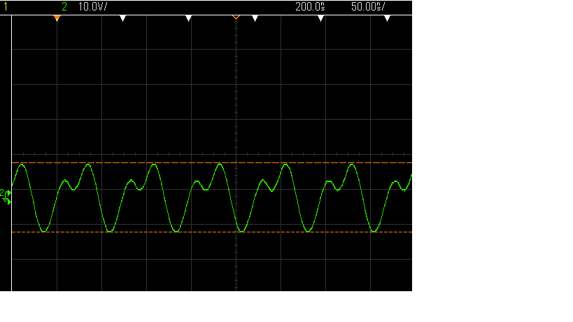
    TP03 Signal (Vpp=19.7V) at 50ohm after impedance matching network(L101/C101/C102/C103) is shown, it is a good sine wave.

    Are they correct signals waveform? How should I adjust these component values if not?

    Thanks.

    Best Regards

    Brian

  • Hi Brian,

    Regarding your question of "Thank you for your support, it works well after porting your firmware on the TRF79XX. It is more robust than the old one I used ever, do you have newer version now?"

    I don't recall anymore which firmware I had shared with you, could you link me to the E2E post or give me the CCS project name? Then I can tell you if there have been any updates to it :)
  • Hi Ralph,
    There is this link in private message with you.
    e2e.ti.com/.../conversations
    This file "TRF7960ATB_G2_RFID_Reader_Demo.zip" was send by you on May 5,2016.
    Thanks
    Best Regards,
    Brian
  • Hi Brian,

    Ahh thanks. Yes, I am working on a newer version of that code still, but it isn't ready to be shared yet. Hopefully within the next couple weeks. I'll let you know when it is.

    There isn't so much changes to the ISO layers as there are a number of TRF79xx driver improvements and tweaks to the application etc.
  • Hi Ralph,

    Ok, thank you for sharing your latest information about firmware. Waiting for your news.

    Thanks.

    Best Regards,

    Brian

  • Hi Josh,

    It seems that it is difficult for you to have time, Could any other engineer in this production area help to feedback my questions?

    Thanks.

    Best Regards,

    Brian

  • Brian - 

    Q1. According to your TRF7970A external power amplifier document, I may simplify this design for 1W RF power output if only using one receiving signal RX_IN1 and 100% modulation transmitting, optional RX filter and external modulation control can be not needed, is it correct?

    A1. Yes, you can use only one RX channel if that works well enough for you in your application. 

    Q2. When transmitting TP05 signal Vpp is 20V, RX_IN1 input resistance in datasheet is 10kohm, Vpp value of input signal is about 10V from calculation(voltage divider resistance 3.9kohm), so it exceeds Maximum RF input voltage at RX_IN1(3.5V). can the TRF7970A chip be damaged?

    A2. Yes, exceeding the specified maximum input voltage on the RX line will damage the IC (like it would on any other device which has maximum input specifications - this is why they are published)

  • Hi Josh,

    Thank you for your feedback, I got your answer for the two questions last time(one week ago), you also attached your simulation circuit. After that I sent some further questions to you, I re-paste them here,

    1. If I use this simulation circuit you attached, is it enough that I configure the registers like this way? 
    i. For Modulator and SYS_CLK Control Register (0x09)
    B6 =0 not use external modulation control 
    B2B1B0 =001 modulation OOK 100% 
    ii. For Regulator and I/O Control Register(0x0B)
    B6 =1 support external power amplifier

    Sorry,I did not understand what you said "still need the variable voltage divider to adjust your depth correctly". 
    Could you explain more about this?

    2. "The complete filter is matched to Zin = (45+j7) input and Zout = (57−j3) output impedance at 13.56MHz" is described in this document, I analyzed impedance transformation from TP03 to TP06 using smith chart tool,impedance at TP06 is 42-j31,it is big different from 57-j3, is there any problem on my analysis?
    for class E power amplifier,C1(150pf)/C2(1040pf)/L2(560nH) can be adjusted to achieve the best efficiency and signal shape according to figure 8 in the document, the value of C1 is different from the one of C100 (100pf) given in your simulation circuit, which value should I use?

    3. 

    I have gotten this board (made according to your simulation circuit), it is a little different from your circuit.

    L101/L104         538nH (replacing 560nH in your circuit)

    L105                  422nH (replacing 390nH  in your circuit)

    Vgs(channel 1: Vpp=7V ) and Vds(channel 2:Vpp=47.8V) waveform is shown, less duty ratio and high peak-peak value comparing to fig 9 in the document

    TP03 Signal (Vpp=19.7V) at 50ohm after impedance matching network(L101/C101/C102/C103) is shown, it is a good sine wave.

    Are they correct signals waveform? How should I adjust these component values if not?

    Thanks

    Best Regards,

    Brian

  • Hi Ralph,
    Josh is very busy, do you know if any other engineer in this product group can help me?
    Thanks.
    Best Regards
    Brian
  • Hi Brian,

    No, we do not support power amplifier designs in this product group anymore, sorry.

  • Thank Ralph.

    Best Regards,

    Brian

  • Hi Brian,

    The updated firmware has been released. You can find the details about the updates here (I updated the bottom half of the E2E post): e2e.ti.com/.../493678
  • Hi Ralph,

    Very good release, thank you for your sharing.  

    Thanks

    Best Regards

    Brian