

This technical article was updated on July 23, 2020.
In my previous blog post, I explained the differences between a SAR ADC’s throughput and response time. Today, let’s see how an interface topology affects the throughput and response time of a SAR ADC.
A typical SAR ADC has two phases of operation, acquisition and conversion, which function as follows:
- During the acquisition phase, the sample-and-hold switch is closed, and the SAR ADC acquires the external analog input on the sampling capacitor. Then, the host controller issues a start-of-conversion (SOC) signal to end the acquisition phase and start the process of analog-to-digital conversion.
- During the conversion phase, the SAR ADC converts the sampled/acquired analog input to an equivalent digital code by employing a binary search algorithm. The digital data output is then transferred to the host controller using the digital interface between the ADC and the host controller.
Here are some helpful definitions to know:
- tTHROUGHPUT: Minimum time difference to be maintained between two consecutive samples, such as between the two SOC signals.
- tCONV: Conversion time – time taken by the ADC to convert the sampled analog voltage to its equivalent digital code.
- tACQ: Acquisition time– time taken by the ADC to acquire an analog input signal.
- tDTX: Data transfer time – time taken by the ADC to transfer the conversion result to the host controller.
- tRESP-ADC: Response time – time difference between host controller issuing an SOC signal and receiving the conversion result.
- tRESP-ADC-m: Response time for m-bit – time difference between host controller issuing an SOC signal and receiving the “m” bits of the conversion result.
tCONV, tACQ and throughput are always explicitly specified in the SAR ADC datasheet. However, it can be quite tricky to find out the data transfer time (TDTX), especially for devices that have a complex/flexible interface.
See below for timing specifications for a typical SAR ADC.
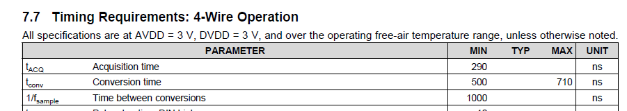
Figure 1: Timing specifications for a typical SAR ADC
Let’s look at different ways of transferring the conversion result back to the host controller and understand how these interface topologies affect tTHROUGHPUT and tRESP-ADC.
Interface Type 1: Data bits are transferred as they are resolved
This is the easiest form of data transfer interface for SAR ADCs and the operation is driven from an externally provided clock. The ADC resolves 1 additional bit per clock provided, and the resolved bit is (almost) immediately transferred to the host controller using the same clock. Figure 2 below shows this type of interface implemented in TI’s ADS7042:

Figure 2: Example of interface type 1
As an example, the ADS7042 has a throughput of 1 Msps (or tTHROUGHPUT = 1 us), but its response time is faster only at 844 ns as defined in the equations below.
- tTHROUGHPUT = tCONV + tACQ
- tDTX < tTHROUGHPUT
- tRESP-ADC = tDTX
- tRESP-ADC < tTHROUGHPUT
Further, if tCLK is the clock period of the external clock and ”n” is the resolution of the ADC, then one new bit of information is available to the host controller after every tCLK time interval (with an initial delay of 2 tCLK).
Therefore:
- tRESP-ADC-1 = 3 * tCLK
- tRESP-ADC-2 = 4 * tCLK
- or in general : tRESP-ADC-m = (m+2) * tCLK (where; m < n)
Where would this be useful?
Consider an example where a control system using the ADS7042 requires the following:
- Input signals in the range 0 to 3*VREF/4 to be resolved to 12-bit accuracy.
- Input signal > 3*VREF/4 to be flagged as an alarm condition as soon as possible.
As you can see, when the input signal is in alarm range, the first 2 bits of ADS7042 output will be 11. As shown in Figure 2, this information is available to the host controller in time tRESP-ADC-2 and hence an alarm can be triggered immediately (without waiting for the conversion process to complete).
When the input signal is in normal range (i.e. the first 2 bits of ADS7042 output are not 11), the host controller provides more clocks to resolve all the remaining bits to get a 12-bit accurate final output code.
Can you think of a limitation of such an interface?
Any error in any of the bit decisions will get transmitted immediately to the host controller and may result in an erroneous control action.
The probability of getting such an erroneous bit decision increases at higher throughputs and also at higher resolutions. Therefore, this type of interface is usually restricted to lower resolution or to lower speed.
In the next post of this series, we will look at two other types of interfaces used by higher precision ADCs (>12 bits), especially at higher throughputs (>100 Ksps).
Additional resources:
Learn more about TI’s ADS7042 ultra-low power and ultra-small 12-bit, 1 Msps SAR ADC with SPI interface, download the datasheet and order samples.
See the Three 12-Bit Data Acquisition reference designs optimized for low power and ultra-small form factor.
Read additional posts in the SAR ADC response times series.
