This thread has been locked.

If you have a related question, please click the "Ask a related question" button in the top right corner. The newly created question will be automatically linked to this question.

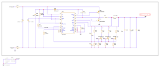
LM5149-Q1: DC-DC 67.2v to 20v/15v/9v/5v ; TCAN1162x ; TPS25750

Part Number: LM5149-Q1
Other Parts Discussed in Thread: LM5149, TPS25750, CSD19533Q5A

Hi,

 I have a question regarding my 16s BMS (Battery Management System) (design).

I intend to use a PD (Power Delivery) Type-C source exclusively for charging purposes, either for phones or PCs...

The battery voltage is 67.2V, and I plan to employ a DC-DC Buck converter capable of delivering 5A .


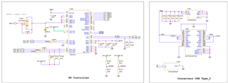
I have a sample schematic for my DC-DC converter and PD (Power Delivery) controller that I would like to share with you.

The purpose of the DC-DC converter is to supply power to a CAN transceiver and charge a USB PD Type-C device with multiple voltage options (5V/9V/15V/20V).

I have selected the TCAN1162 due to its voltage supply range of 5.5V to 28V. However,

I am unsure whether my design is correct or not.
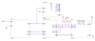


I would greatly appreciate it if you could review the schematic and provide any remarks or suggestions for improvement.

Your expertise in this field would be invaluable to ensure the effectiveness and reliability of the design.

Thank you in advance .

I look forward to your feedback.

Best regards,
Ahmed.

  • Hi Ahmed,

    Thanks for your inquiry. I can only provide feedback for the LM5149 device. While I take a look at your schematic, could you please fill out this quickstart with your design parameters?

    Regards,

    HenryLM5149-LM25149 Quickstart Calculator_rev3.xlsm

  • Hi Henry Kou, 

    Thank you for your response.

    The Excel document you provided has been really helpful(about DC-DC With LM5149) , and it has given me more information.

    Do you have any additional feedback on the PD controller schematic?

    Thanks 

    best regards,

    AHMED. 

  • Hi Ahmed,

    I would recommend creating another E2E post with reviewing just that part, TPS25750, so that the appropriate team can cover it.

    As for the LM5149 device schematic, here are my notes:

    • Add damping capacitor for supporting line transients and input filter: https://www.ti.com/lit/pdf/slyt670
    • Add more ceramic CIN capacitance >40uF (derated)
    • Enable, PG, VCCX, ISNS, CNFG connections seem good.
    • Set frequency of ~150kHz with RT seems a bit low, recommend switching to 2.1MHz or 1MHz, see attached recommended spreadsheet calculator bode plot.
    • Omit R811 pullup for EXTCOMP
    • Omit D80D diode from VCC to CBOOT
    • For Feedback network, refer to attached document for dynamic Voltage output setting with the switches option.
      • 20V feedback network seems to correlate to an output voltage of 26V. Recommend R812 to be 190k, R817 to be 10k.
    • Refer to the attached recommended spreadsheet calculator for choosing recommended compensation values for achieving stable operation at each VOUT setting.
    • For the switching FETs I would recommend different ones for the following reasons:
      • Miller plateau for CSD19533Q5A is not sufficiently within 2V - 3V range, so FET will not be switching properly
      • RDS_on value for VGS = 4.5V can be very high
    • Instead, I recommend ISC0602NLSATMA1 or another NFET similar. I've input the parameters from the datasheet onto the recommended spreadsheet.

    Regards,

    Henry

  • Hi Henry Kou, 

    I appreciate your feedback and the time you've dedicated to this matter.

    The file you provided has been quite helpful to me, but I do have a few questions.

    Referring to the file.xlsm, if I select a frequency of 2.1 MHz, the power dissipation increases, and the junction temperature exceeds 160°C. This is because VCCX is connected to GND( as I do not have an external 5V supply in my design) . That's why I have opted for a frequency of approximately 400 kHz.

    For R811, I have chosen a value of 100kΩ as indicated in the design referred to as Calculator.xlsm(, which you shared,) for internal compensation.

    Regarding the file.pptx (Dynamic output voltage change) and the datasheet, the following formulas apply:

    Rfb1 = (Vout/Vref - 1) × Rfb2

    Vout = Vfb × (1 + Rtop/Rbot)

    Vref = 0.8V

    By substituting the values:

    0.8 × (1 + 249/10) = 20.72V

    (Considering there is a diode in my design with a voltage drop of approximately 0.5V, that's why the voltage is around 20.72V instead of 20V.)

    I would like to understand why the value of 190kΩ is recommended instead of 249kΩ?

    (The recommended starting value for Rfb2 (Rbot) is between 10 kΩ and 20 kΩ.) 

    That's why I chose to fix Rfb2 at 10kΩ and make Rfb1 dynamic. However, in the file.pptx (dynamic output voltage), it suggests fixing Rtop and making Rbot dynamic. If I choose this configuration, Rfb2 will fall outside the recommended value range mentioned in the datasheet. Is there a significant difference between these two configurations? And which one is better? 

    Thank you for addressing the other points. I will take them into consideration.

    Once again, I appreciate your guidance, feedback, and the time you took to respond.

    Best regards,

    Ahmed. 

  • Hi Ahmed,

    Actually I see what you are saying. I do agree with you on the following:

    - Operation at 400kHz is fine as long as the compensation can ensure stability for the system at the different Voltage outputs.

    - At 20Vout, RFB1 should be 249K, and dynamic Rtop method will work equally as fine.

    Regards,

    Henry

  • Thank you Henry Kou, 

    This resolved my issue, 

    Best regards, 

    Ahmed.