This thread has been locked.

If you have a related question, please click the "Ask a related question" button in the top right corner. The newly created question will be automatically linked to this question.

TPS7A20: A phenomenon in which the output voltage is not 0V when VEN=0

Part Number: TPS7A20
Other Parts Discussed in Thread: TPS7A26

Tool/software:

hello. In this project, the circuit was constructed using TPS7A20.

The current consumption of the load connected to the TPS7A20 does not exceed 10mA.

I am trying to turn the TPS7A20 output ON/OFF by controlling the VEN on the FPGA.

When VEN=0, Vout is output as an abnormal voltage instead of 0V(1.55V)

I would like to know why this phenomenon occurs and what solutions might be available.

Due to internal security policies, I cannot provide the complete circuit. Therefore, I am attaching a portion of the schematic that includes the TPS7A20.

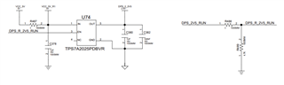
The attached oscilloscope capture shows the state of the board when power is applied. (Green = VIN(5V), Blue = VOUT(1.55V), Yellow = VEN).

I suspect that the issue might be that, despite VEN being 0, the output is showing 1.55V, which seems to be the UVLO voltage being connected to the output. Please review this as well.

For additional information, when VEN is High, the output is 2.5V (normal operation).

  • Hello,

    I am working on finding a solution to this problem. I realize that this is the second problem of this type which you have observed recently, both with different devices.

    Could you please let me know if there are commonalities in these circuits/ testing methodologies which may be causing these issues? Meanwhile I will debug with the information you have sent.

  • Yes, that's correct. I am using the TPS7A26 and TPS7A20, and I am experiencing an issue where an unexpected output voltage appears when VEN=Low.
    The common factor is that the output voltages are connected to a device from ADI, the AD5560.
    To debug whether the issue is caused by the ADI AD5560, we tried to disconnect the output of the TPS7A20 from the ADI AD5560 input voltage and check, but the board remains shorted, so it is unclear which device is causing the malfunction.
    In this project, we have produced 20 boards, each using 2 TPS7A20 and 2 TPS7A26 (a total of 40 TPS7A20 and 40 TPS7A26). We are experiencing the same issue with all 80 devices.
    If the devices are damaged, EN control should not work properly or unexpected output voltage should appear in the EN state. However, EN control and output voltage are working correctly (except for the fact that 0V does not appear when EN=Low).
    We need to produce many more boards, but production is currently halted due to this issue. We need a prompt response as soon as possible.

    Thank you for your understanding..

  • Could you please show me how the AD5560 is connected to the TPS7A26 and TPS7A20 in the schematic and also the layout of these parts? I want to check for any coupling of voltages to the EN node.

  • 1.Attached is the schematic of the AD5560.

    A 100nF decoupling capacitor is connected in front of the AD5560 input for the TPS7A20.

    A 10uF (1ea) and 100nF (3ea) decoupling capacitors are connected in front of the AD5560 input for the TPS7A26.

    Two AD5560 devices are connected per device (TPS7A20, TPS7A26).

    Additionally, to verify if the connected open-drain pull-ups on the AD5560 were causing the issue, we removed them all, but the voltage when VEN=Low on the TPS7A20 remained at 1.55V.

    If you need additional information, please let me know.

  • Hi,

    This device has a smart enable circuit to reduce quiescent current. When the voltage on the enable pin is driven above VEN(HI), as listed in the Electrical Characteristics table, the device is enabled and the smart enable internal pulldown resistor (REN(PULLDOWN)) is disconnected. When the enable pin is floating, the REN(PULLDOWN) is connected and pulls the enable pin low to disable the device. 

    I suggest the following steps for this debug:

    1. Please perform an ABA swap to see if the problem persists
    2. While the device is disabled, please probe EN and confirm that it is in a LOW state.
    3. The AD5560 is not a TI part so I cannot advise on whether the EN signal it generates is high impedance during TPS7A20 disable. Please confirm what 'DPS_2V5_RUN' is and probe it.

    We can suggest next steps after the above information is received.

  • 1. I already conducted an ABA SWAP, and the issue remains the same.

    2. I first captured and uploaded the oscilloscope screen, which shows the waveform of VEN. The low state is certain.

    3. I'm not seeking advice about the AD5560; you asked about the connection parts of TPS7A20 and TPS7A26, so I provided the information. I used the TPS7A Series, and the only connection is with the AD5560. If it's unnecessary, I'll delete the response for security reasons. 'DPS_2V5_RUN' is a signal that controls the TPS7A20 from the CPLD, and there's no problem with H and L Control. By controlling VEN, 2.5V is output when High, and 1.55V is output when "VEN is Low."

    This has all been confirmed in 1, 2, and 3. What is next step?

  • If the above steps did not work, then I assume that there is a leakage path on the board. Please share the board file and a picture of top and bottom of the assembled board

  • Due to company security reasons, I cannot share the board file. However, I will capture and share all parts connected to TPS7A2025. In the explanation of the picture below, the Output net of TPS7A2025 is marked in red, and it is confirmed to branch into Decap, Pull-up, Mux input, and Test point. I am sharing the results of checking for leakage points.

    1. Decap - Almost no probability of leakage path.

    2. Pull-up - Even after removing all pull-ups and performing an ABA Swap, the same phenomenon occurs.

    3. Mux input - Open state as it is not measuring the voltage of TPS7A2025 with the mux having 32 channels.

    4. Test point - Open point for DVM measurement.

  • Please refer to this snapshot from validation process for the above device. The blip that is seen in your measurements is absent here. 

    What it looks like is happening is that the output in your circuit is being back fed, and once the input voltage reaches the UVLO level or at least enough to turn on the active pulldown, the output is discharged by the pulldown

  • First, I will explain what I understand about the TPS7A20. Please point out any errors in this explanation.

    • The TPS7A20 turns off the MOSFET output when the input voltage is below VUVLO (1.17~1.59).

    • The TPS7A20's active discharge is enabled when VEN is low or when the input voltage is below VUVLO.

    Therefore, in the power-on condition of my current circuit, since VEN is always low, the active discharge is enabled.

    I have two hypotheses regarding the cause of the unexpected voltage output issue in this state:

    1. Is it correct to assume that when the MOSFET is off, backfeeding occurs through the discharge resistor at the output pin (10.3 mA = 1.55V/150Ω)?

    2. I suspect that the unexpected output (1.55V) is caused by a short circuit between the VUVLO voltage and VOUT. Could you please review if this possibility exists?

  • 1. I do not see this discharge resistor on the output pin. Could you please identify it for me? If present, yes that would be a very probable path for backfeed.

    2. VUVLO is the voltage at the input at which the output drops. A short circuit between the VUVLO voltage and VOUT would mean an IN to OUT short. Nevertheless, I will ask Systems team if this is a possibility that can lead to a similar failure for this device.

    1. The TPS7A26 has an internal discharge resistor (150 ohms). This is mentioned in the datasheet.

    2. I think that VUVLO is not the same voltage as VIN but rather a circuit that compares VIN to the VUVLO voltage and applies a lock. Therefore, it does not seem to be the same voltage as VIN. Could you please confirm if my understanding is correct?

  • 1. That is correct

    2. The node labeled in red holds the voltage seen by the internal logic controller to determine UVLO.

  • It is assumed that the block labeled UVLO contains a comparator that compares the input voltage with the reference voltage of UVLO. It is also assumed that VUVLO and VIN are compared, and the result (H/L) is sent to the internal controller to determine the ON/OFF state of the output MOSFET.

    Since a voltage identical to the reference voltage of UVLO (VUVLO) is being output at VOUT (1.55V), I raised Question 2 regarding this matter.

    My question is whether there is a possibility of a short circuit between VUVLO and the output. I need a definitive answer as to whether there could be another cause for this issue beyond backfeeding current into the output pin.

  • Thank you for the clarification. Yesa, your analysis is absolutely correct. There is a possibility of a short circuit between VUVLO and the output but this is highly unlikely. We have not noticed similar failures for this device in the recent past. This leads me to believe that the issue could be current backfeeding from OUT to IN.

    If you would like me to examine the issue in lab, please ship me some of the faulty units, some control units from the lot and if possible, one of your populated circuit boards. I will try to recreate the fault in our lab. Please drop your email here so I can contact you with shipping address and instructions.

  • First of all, thank you for taking the time to answer my questions over such an extended period.

    To address the issue, I will assume that the unexpected behavior is caused by backfeeding through the OUT pin and the discharge resistor. As a solution, I plan to use a product without a discharge resistor to avoid such problems.

    Unfortunately, due to company security regulations, it is not possible to take the board outside the company, so analyzing it in the lab will not be feasible.

    Thank you again for your support.

  • You are welcome