Other Parts Discussed in Thread: TIDA-010247
Tool/software:
Hello,
We have a strange behaviour in our design which is very similar to TIDA-010247..
The board is connected to a cell simulator fixture (20 cells - 10 for each BQ) and powered by 48V supply.
The FETS and and current sensing resistance are NOT CONNECTED yet.
We are seeing strange voltages on Stack voltages which are NOT EQUALS to the sum of cell voltages and the values themselves should be 24V for each BQ.
It is notable that lowering supply voltage to 24V causes the gap to disappear
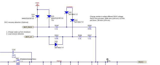
Here is screenshot from our custom monitoring tool:
(Left column is BOTTOM BQ and right column TOP BQ)
Power suppy at 49V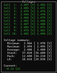
Power supply at 36V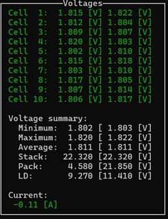
Power supply at 24V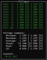
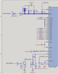
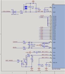
Here are the relevant schematcis:
Any ideas on what is happening here?
Thanks Vadim