

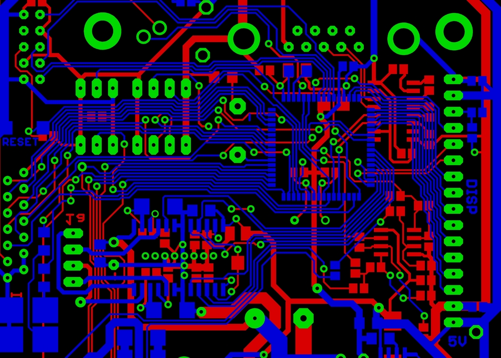
After a design’s schematic and bill of materials (BOM) are finalized, the design proceeds to the printed circuit board (PCB) layout phase. While the layout takes a significant amount of time to do correctly, this is often the point in the project where the schedule becomes compressed and rushed. You’ll hear, “Get that board out!” for the few days or weeks that a project is in layout. Don’t make the mistake of skipping the PCB layout step because of time pressures.
While the schematic and BOM dictate some portions of the circuit’s performance, the PCB layout can make or break a good schematic and BOM. For example, excessive trace length or narrow trace widths can turn a capacitor into an inductor due to the parasitic inductance in such traces. Would your schematic pass its review if all the capacitors were inductors? Because it is so important, you should do a PCB layout review on each and every circuit, on every PCB revision.
A good PCB layout reviewer should be knowledgeable about the circuit type they’re reviewing. For power supplies, this is someone with experience designing power supplies. Knowledge of thermal issues is important too, such as power-dissipation capabilities of a component and temperature rises and parasitics from components and PCB layout.
You should budget time in the PCB layout process to review the layout, implement the required changes and then re-review the new layout. The time you spend now can save hours, days and weeks of frustration later. In many cases, a PCB layout review saves a future PCB spin, which is a huge time and cost sink for any project.
I go through an example PCB layout review in detail here, but the key questions to ask are:
- Is the input capacitor placed as close as possible to the IC’s (P)VIN and (P)GND pins and routed directly to those pins? Is there any possibility to make this capacitor be closer to those pins?
- Is the SW node as small as possible with the inductor close to the IC?
- Is the output capacitor placed close to the VOS pin on DCS-Control devices and (P)GND on all devices?
- Is the FB node as small as possible with the resistors and capacitors connected to that pin located close to the IC?
- Are any sensitive analog circuits, such as the FB network, located near the inductor?
- For non-Wafer Chip Scale packaged devices (WCSPs), are sufficient thermal vias under the device?
PCB layout reviews are extremely important. They improve the performance of circuit designs, prevent component failures, and save wasted time fixing PCB layout issues.
How have PCB layout reviews saved your designs from unplanned board spins?
Additional resource
- WEBENCH® software tools to help speed your time to market
-

Ahmet Cetin
-
Cancel
-
Up
0
Down
-
-
Reply
-
More
-
Cancel
Comment-

Ahmet Cetin
-
Cancel
-
Up
0
Down
-
-
Reply
-
More
-
Cancel
Children