

A common request from customers in the E2E community is for a “schematic review.” This review also may be called “checking my circuit” or “validating my design.” What is a schematic review, and why is it important? How do you do a review, and are there any tips that everyone can benefit from?
A schematic review should be done on every circuit. Most of you are doing reviews already, but you may not know it. A review is simply to have someone other than the circuit designer take a look at the design and check it for errors before the design goes to layout. This review can be done by a manager, co-worker, applications engineer, or system engineer. A good review involves more steps. It requires a reviewer who is knowledgeable in the circuit to review the design. Example: With the power supply circuits that I support, the reviewer should be a power supply designer or at least an analog engineer. Having experience with the circuit type is important to catch errors. In a project’s design phase, a review of the schematic, bill of materials (BOM), and printed circuit board (PCB) layout is critical to catch errors when they are on paper and not in built hardware. Time spent now is well rewarded with less time debugging and fixing hardware later.
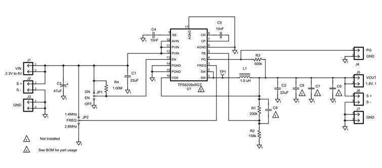
Doing a schematic review requires system knowledge of the operating circuit. First, check the operating parameters of the system, such as input voltage range and output voltage setpoint and accuracy as required output current. Second, compare the data to the IC datasheet’s recommended operating conditions. Example: Look at the data below from the TPS62085 datasheet.
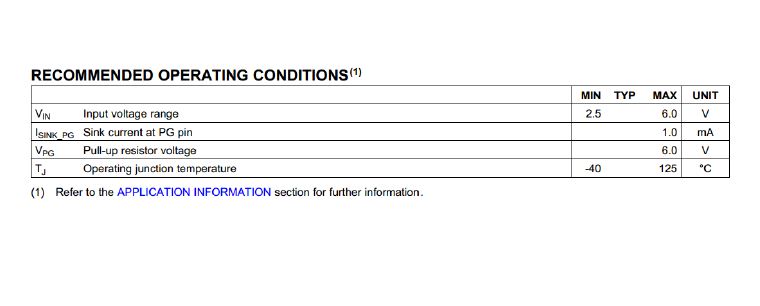
Note footnote 1 above tells you to the read the Applications Information section of the datasheet. This section shows you the recommended circuit and explains the external component requirements. The datasheet guidelines and requirements should be followed to ensure a working design. If they are not, ask the circuit designer why he or she deviated from the guidelines. Be sure to ask your applications engineer if this change is acceptable. With the highly integrated TPS62xxx family of devices, the external components have already been optimized for size, efficiency, and cost, so there is rarely a reason to deviate from the requirements in the D/S except in very special circumstances. Once your feedback has been discussed with the circuit designer and/or an applications engineer, the schematic review is done.
Here are some key things that I always check in my reviews:
- Is the best device chosen for the system operating conditions?
- Do the component values for Cin, Cout, L, etc. match the values in the typical application schematic in the datasheet?
- Are all the grounds connected to the same node?
- Are all the pins terminated? If any are floating, is this allowed?
Hopefully, these tips have been helpful to you. Look for my future posts over the next few months on BOM and PCB layout reviews in Fully Charged.
How have schematic reviews saved your designs from non-working hardware?
