

Power banks are popular personal accessories for portable electronics like smartphones or tablets, whose stylishly thin profiles mean limited battery capacities. A power bank is a portable secondary battery that stores energy when alternating current (AC) power is not available.
Figure 1 is a power-bank operation board with two USB ports. One port is mini USB, connecting the power bank to a USB charging adapter to store energy in the power bank. The other USB port is a standard Type-A USB port for charging smartphones or tablets on the road.
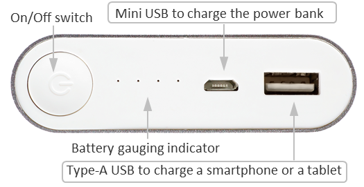
Figure 1: Power-bank operation board
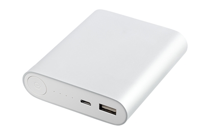
Depending on the form factor and budget, a power bank can use different battery cells. Figure 2a shows a power bank with several thousand milliamp hours (mAh) battery capacity for smartphones. It uses lithium-polymer (Li-polymer) battery cells to achieve a thin form factor. Another type of power bank with tens of thousands mAh battery capacity, generally uses 18650 batteries (cylindrical cells 18mm in diameter and 65mm high) to achieve high charging capacity at a reasonable cost. Figure 2b is an example of such power bank with multiple 18650 cylindrical packs in parallel inside the case.

(a)
(b)
Figure 2. Power bank with different form factor
The form factor of a power bank determines size and capacity of a power bank. There are also many other technical considerations in the development of a power bank. Table 1 lists the basic application requirements and technical challenges for power banks from battery charging and discharging perspectives.
|
Application requirements |
Technical challenges |
|
Mobility and flexibility |
High integration with host control option |
|
USB D+/D- detection |
Advanced digital-circuit design technology |
|
Long battery life and backup times |
High battery charging voltage accuracy and high boost power-conversion efficiency |
|
Voltage based battery gauge function |
Integrated ADC for voltage-based battery capacity gauging |
|
Low electromagnetic interference (EMI) |
Optimized switching-cycle performance and IC/PCB layout |
Table 1: Power-bank application requirements and technical challenges
Figure 3 is a block diagram of a two-stage power bank; this is one of the most straightforward solutions. The first stage is a single-cell battery charger, which could be either a linear charger such as the bq24090 or a switching charger. The advantage of the linear charger is its low cost, low EMI and small solution sizes. For high-capacity power banks from several thousand milliamp hours up to 10,000mAh, switching chargers are necessary to reduce charging times with low temperature rise. The second stage is a boost converter such as TPS61088 to step up the battery voltage to USB-compliant 5V, depending on the output current and cable resistance. Two sets of switches and inductors perform charging (red trace) and boost (blue trace) separately.
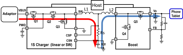
Figure 3: A power bank with two conversion stages
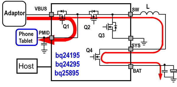
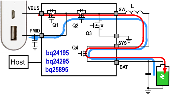
The two stages approach requires two sets of switches and inductors to perform buck charging and boost on-the-go (OTG), which increases the total solution cost. Single-chip fully integrated power-bank ICs, like the bq24195 and high voltage fast charging bq25895, require only one set of switches and an inductor to perform both charging and boost functions. Figure 4a shows the power-bank charging mode (red thin trace) and bypass mode (red wide trace).
When the adaptor mini-USB cable is plugged into the power bank, the charger initiates the D+D- detection to determine the input current capability and set the charger input current not to exceed the detected value. If the device is attached to a Type-A USB terminal via cable, the adapter current will guarantee the bypass phone charging (thick red line on Figure 4a) as a high priority due to the input current dynamic power management function of a charger – only the remaining extra power will charge the battery.
The blue trace on Figure 4b shows a power bank operating in OTG boost mode. The adapter is unplugged and the battery voltage is boosted to around 5V to charge the phone. The set of switches and inductor used to operate in buck-charging mode now operate in boost-discharging mode to charge the phone; no extra components are required, thus reducing cost.
To enable the battery to charge and discharge, the battery temperature is sensed by a negative temperature coefficient (NTC) resistor not only during the charging mode for all three chargers but also during the discharge boost mode for bq24295 and bq25895 to ensure the desired operation of the battery.
(a)
(b)
Figure 4: Power-bank bypass and charging mode (a) and OTG boost mode (b)
As you can see, the family of single-chip fully integrated power-bank ICs presented in this blog has only one set of switches and inductor. The bq25895 integrated ADC can be used with the host for battery capacity gauging. The solution simplifies designs and keeps BOM costs low, while satisfying many of the challenges of designing power banks including high integration for mobility, D+D- detection for input current limit, and battery temperature sensing in both charging and discharging modes for desired temperature operation range. Start your power banks design process by taking a look at the TI Designs below.
Additional resources
- Check out these TI Design reference designs that use the bq24195, bq24195L and bq25895battery charger ICs:
- I2C Controlled Single Cell Chargers with 5.1V Boost Operation: bq24195/2.1A and bq24195L/1A.
- I2C Controlled Single Cell 5A Fast Charger with MaxCharge and 3.1A Boost Operation for Power Ban.
- Learn more about designing power banks with the TPS61088 in the blog post:Smaller, more efficient power banks coming your way!
-

AIGun
-
Cancel
-
Up
0
Down
-
-
Reply
-
More
-
Cancel
Comment-

AIGun
-
Cancel
-
Up
0
Down
-
-
Reply
-
More
-
Cancel
Children