

This technical article was updated on July 23, 2020.
When designing a high-performance data acquisition system, a diligent engineer carefully selects a precision analog-to-digital converter (ADC) and the additional components needed for the analog front-end conditioning circuit. After spending weeks designing, performing simulations and optimizing the schematic, the designer quickly puts board layout together to meet a tight deadline. A week later, the first prototype board is tested. To his or her surprise, the circuit does not perform as expected.
Has this ever happened to you?
Optimal PCB layout is essential to obtain the expected performance of your ADC. When designing circuits with mixed-signal devices, you should always start with a good grounding scheme and partition the design into analog, digital and power sections using optimal component placement and signal routing.
The reference path is the most critical in ADC layout, because all conversions are a function of the reference voltage. With a traditional successive approximation register (SAR) ADC architecture, the reference path is also the most sensitive, as the reference pin presents a dynamic load to the reference source.
Since the reference voltage is sampled several times during each conversion, high-current transients are present in this terminal where the ADC’s internal capacitor array is switched and charged as the bit decisions are made. The reference voltage must remain stable and settled to the required N-Bit resolution during each conversion clock cycle, or linearity errors and missing code errors may occur.
Figure 1 shows the current transients during the conversion phase on the reference terminal for a classic 12-bit SAR ADC.

Figure 1. Current Transients on the Reference Pin of a 12-Bit SAR ADC
Because of these dynamic currents, the reference pin requires good decoupling using a high-quality bypass capacitor (CREF). The bypass capacitor is used as a charge storage reservoir that can provide instantaneous charge during these high-frequency transient currents. You should place the reference bypass capacitor as close as possible to the reference pin and connect them using short, low-inductance connections.
Figure 2 shows a board layout example for the ADS7851, a 14-bit, dual ADC with two independent internal voltage references.
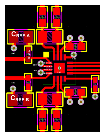
Figure 2. Layout example for a Dual ADC with Two Independent Internal References
In this four-layer PCB board example, the designer used a solid ground plane right underneath the device and partitioned the board into analog and digital sections keeping the sensitive inputs and reference signals away from noise sources. He bypassed the REFOUT-A and REFOUT-B reference outputs with 10-μF, X7R-grade, 0805-size ceramic capacitors (CREF-x) for optimal performance and connected them to the device using small 0.1-Ω series resistors to keep the overall impedance low and constant at high frequencies. He also used wide traces to reduce inductance.
I highly recommend placing CREF in the same layer as the ADC. You should also avoid placing vias between the reference pins and the bypass capacitors. Each reference ground pin of the ADS7851 has an independent via connection to GND, and each bypass capacitor has its own low inductance connection to the ground path.
If you’re using an ADC that requires an external reference source, you should minimize the inductance in the reference signal path – starting from the reference buffer output to the bypass capacitor to the ADC’s reference input.
Figure 3 shows a layout example for the ADS8881, an 18-bit, SAR ADC using an external reference and buffer. The designer kept the inductance between the reference capacitor and the REF pin less than 2 nH by placing the capacitor within 0.1-inches from the pin and connecting it with wide 20 mil traces and multiple 15-mil grounding vias. I recommend a single, 10-uF, X7R-grade, 0805-size ceramic capacitor with at least a 10-V rating.
The trace length from the reference buffer circuit to the REF pin was kept as short as possible to ensure fast settling response.
Proper decoupling of the REF pin is critical to achieve optimum performance. In addition, keeping low inductance connections in the reference path allows the reference driving circuit to remain stable and settled during the conversion phase, getting you one step closer to obtaining your desired results.
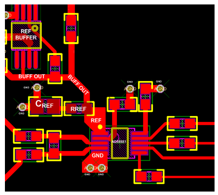
Figure 3. Layout example for an ADC with an External Reference and Buffer
For a deeper look into this topic, check out the Layout Guidelines provided in the ADS8881 and ADS7851 datasheets.
Get more tips from our SAR ADC blog series including:
