

Part 2 of 2:
Two commonly asked questions when designing an operational amplifier into a new application are:
1. What is its “typical” power dissipation? Covered in my first post.
2. What is its “maximum” power dissipation?
The op amp’s maximum power should be evaluated in the intended circuit. Let’s assume the first case where the amplifier is being operated as such. Let’s load the output with the lowest load resistance RL, as listed in the OPA 316 Electrical Characteristics table. The table lists 2 kΩ (red oval).

Maximum power dissipation will occur when VS and IQ are at maximum and the output is biased to a dc level half the Vs+ supply voltage. Figure 2 shows the OPA316 configured as a single-supply, non-inverting amplifier. Its output is driving the equivalent of a 2 kΩ load to ground, consisting of RL in parallel with the series RF and RI combination. The non-inverting input is driven by a +1.375 Vdc source appearing as 2.75 V at the output due to the 2x gain. One of the OPA316’s output transistors sources current through the 2 kΩ equivalent load resistance, RL(EQV), to ground. It has 2.75V across its source and drain.

Watch our TI Precision Labs video
| In this video, you'll learn the relationship between power and temperature in op amps, including power dissipation at DC and AC, the thermal model of an amplifier and more. |
This TI Precision Labs - Op Amps Series training video addresses relationship between power and temperature in operational amplifiers. In this video, we’ll discuss the power dissipation of amplifiers at DC and AC, describe the thermal model of an amplifier and use it to calculate the amplifier’s junction temperature, and describe the absolute maximum temperature ratings of the amplifier as well as its internal thermal protection schemes.
Figure 2 shows a circuit used for determining the OPA316 power dissipation.
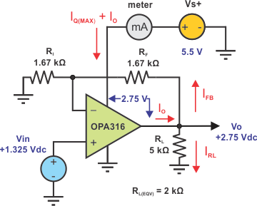
Figure 2: OPA316 power dissipation when driving 2 k-Ohm (eqv.) load
The amplifier power dissipation is calculated as follows:
Find IO the current delivered to the load VO = 2.75 V, RL = 5 kΩ, RF = 1.67 kΩ, Ri = 1.67 kΩ
IO = IRL + IFB = (VO/ RL) + [VO/ (RF + Ri )] = (2.75 V/ 5 kΩ) + [2.75 V/ 2(1.67 kΩ)]
IO = 550 uA + 832.4 uA = 1.373 mA
Iq(max) = 500 uA (from the data sheet)
PD(max) = [(Vs+) * Iq(max)] + [((Vs+) - VO) * IO] = [(5.5 V) (500 uA)] + [(5.5 V - 2.75 V) * 1.373 mA] = 6.5 mW
The power dissipation is quite low and only about 3.2x the quiescent level. This might not be the worst-case dissipation scenario the user is looking for, but it is a good starting place.
The worst case often occurs when the output is shorted to ground, or to a supply rail. Modern op amps, like the OPA316, are specified and capable of withstanding an output short to ground without being damaged. The OPA316 short-circuit information is listed in the data sheet Absolute Maximum Ratings table.
The output current IO is not unlimited, but has a limited short-circuit current value, ISC; the maximum current that the amplifier can deliver with a short to ground. Internal output transistor characteristics and the circuit design dictate the ISC. The Electrical Characteristics, table shown above, lists the OPA316 ISC as ±50 mA (blue oval).
Since the output is forced to 0V, no current flows through the feedback path resistors, or RL. All circuit power is dissipated internally by the OPA316. Figure 3 shows a short circuit connection. Note that the full 5.5 V supply voltage is imposed across the output transistor that sources the ISC current. Its power dissipation PD(XSTR), can be significant.
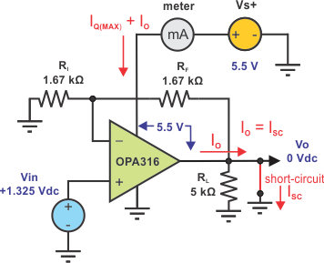
Figure 3 - OPA316 in output short-circuit condition
The op amp PD is now calculated with the output shorted:
IO = ISC ≈ 50 mA
PD(XSTR) = V(XSTR) ∙ ISC = 5.5 V (50 mA) = 275 mW
PQ(MAX) = (Vs+) IQ(MAX) = 5.5 V ∙ 500 uA = 2.75 mW
PD(MAX) = PQ(MAX) + PD(XSTR) = 2.75 mW + 275 mW = 278 mW
This PD level is 43x that obtained from the linear dc load example.
But is the amplifier okay in this case? A calculation of the transistor junction temperature, Tj, should tell us:
Tj = Ta + PD∙θja
Ta = ambient temperature, typically 25 °C
θja = junction to thermal resistance, 263 °C/W
θja value listed in OPA316 Thermal Information table for SC70-5 package
Tj = 25 °C + (0.278 W)(263 °C/W) = 98.1 °C
This is well below the 150 °C Tj maximum that the data sheet lists. The op amp should be okay. Likely the only way Tj could approach 150 °C is if Ta was 50° higher.
Simple dc analysis techniques can help a user understand the power dissipation of an operational amplifier used in their application circuit. The data sheet often provides everything that is needed to perform the calculations. Power dissipation determination involving ac signals is more complex because of the time element. Such analysis usually involves applying integration techniques. Often, however, a dc analysis will provide the worst-case dissipation information.

