

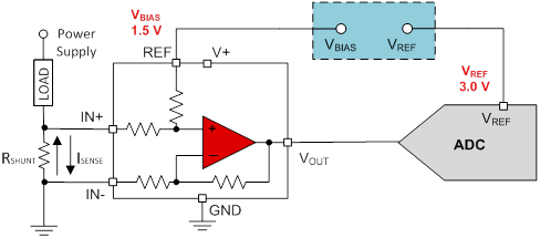
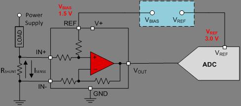
Developing a low-drift system can be very difficult, especially with a bipolar input signal. Applications such as bidirectional current sensing shown in Figure 1, require the use of two well-matched, low-drift reference voltages. The first voltage, VREF, defines the full-scale range of the ADC. A bias voltage, VBIAS, is necessary in order to level shift the bipolar signal. It is desirable to have VBIAS = VREF/2 so that there are equal positive and negative swings for the ADC. I’ll discuss the three topologies for generating two reference voltages in this three part series.
Figure 1: Low-drift bidirectional single-supply low-side current sensing system
Using two separate voltage references, as shown in Figure 2, provides a straightforward approach.
Figure 2: Solution 1 (two separate references)

For the application in Figure 1, VREF and VBIAS are 3.0V and 1.5V, respectively. Table 1 lists a couple of low-drift references. Considering drift, accuracy, and cost, the REF5030A is a good option for the 3V reference voltage. Unfortunately, a low-drift, fixed 1.5V reference is not readily available. In this case, you might select a 1.25V reference, such as the LM4140B, though this unbalances the positive and negative ranges.
Table 1: Low-drift Voltage References

A secondary solution is possible, given a 3V voltage reference using the voltage divider as shown in Figure 3.
Figure 3: Solution 2 (reference + voltage divider + buffer)
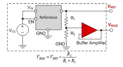
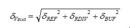
Here, the drift of VBIAS, as shown in Equation (1), comes from the drifts of the reference (δREF), resistor divider network (δRDIV), and buffer amplifier (δBUF).
For a comparable low-drift solution, select resistors with 0.1% tolerance and 5ppm/°C temperature drift. Considering the full-scale range for the amplifier is 1.5V, the offset of the buffer amplifier is not significant. Targeting 0.1% error due to input offset voltage and 1 ppm/°C drift error, the amplifier should have less than 1.5 mV offset voltage and 1.5 µV/°C drift. Table 2 shows the devices selected for this solution. For more detail on component selection, please refer to TIPD156, a current sensing reference design from the TI Designs Precision library.
Table 2: components for second solution

Take a quick look at the two solutions proposed here:
- Solution 1 is a straightforward approach, but restricted to fixed reference outputs and VBIAS is not necessarily VREF/2.
- Solution 2 uses only one reference, so the drift of VBIAS will track with the drift of VREF. Since the resistor can adjust accordingly, this solution has great value when VBIAS ≠ VREF/2. On the downside, this solution requires more components.
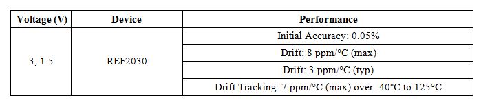
Figure 4 shows a third solution that uses a dual-output voltage reference (REF2030) to offer both the VREF and VBIAS from one chip. Two independent buffers generate the VREF and VBIAS from the band-gap voltage. The internal resistors are sized such that VBIAS = VREF/2. Table 3 lists the main specifications of the REF2030.
Figure 4: Solution 3 (Dual-output reference voltage- REF2030)
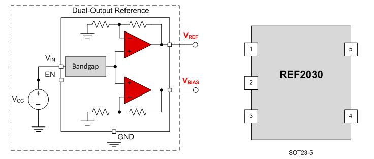
Table 3: REF2030 specifications
So far we’ve shown the three topologies to generate two reference voltages. Stay tuned next week, when we’ll compare the performance of these three solutions.
Resources:
- TIPD156: Low-Drift Bidirectional Single-Supply Low-Side Current Sensing Reference Design
- Part 2: A voltage reference dual of duels


