

In the last two posts in this series I talked about how to build 3-wire analog outputs and how to protect them from transient overstress. This post will finish off the discussion of 3-wire analog outputs with some solutions to one more application-specific problem.
A growing trend in the industrial application space is for analog output modules to provide both voltage and current outputs on a single terminal block. This saves manufacturers some of the costs associated with expensive connectors and cabling. Additionally, this gives a single analog output module the flexibility to serve in virtually any application that requires an analog output.
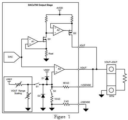
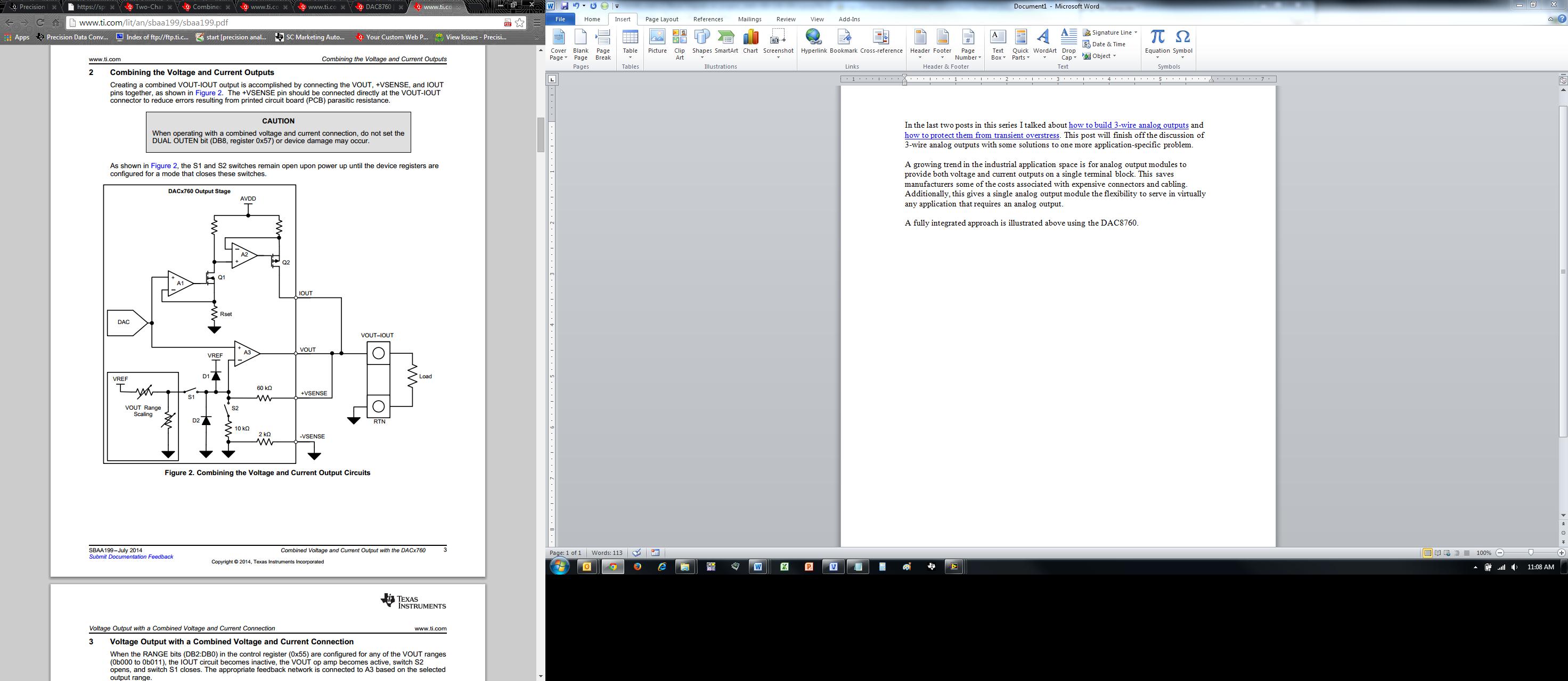
A fully integrated approach, illustrated above in Figure 1, uses the DAC8760 where the VOUT and IOUT terminals are directly connected to one another and the output terminal.
When the voltage output is enabled and the current output is disabled, the IOUT terminal goes to a high impedance state. Since the IOUT pin is high impedance a majority of the output current will flow into the load, allowing the voltage output to perform as specified in the datasheet.
However, when the current output is enabled and the voltage output is disabled, the voltage output buffer (A3) becomes inactive and switches S1 and S2 are opened. This allows for the current output to perform as specified in the datasheet until the voltage potential developed at the high-side of the load is higher than VREF. When this happens diode D1 is forward biased and begins to conduct, sapping current away from the load and creating additional errors for the current output.
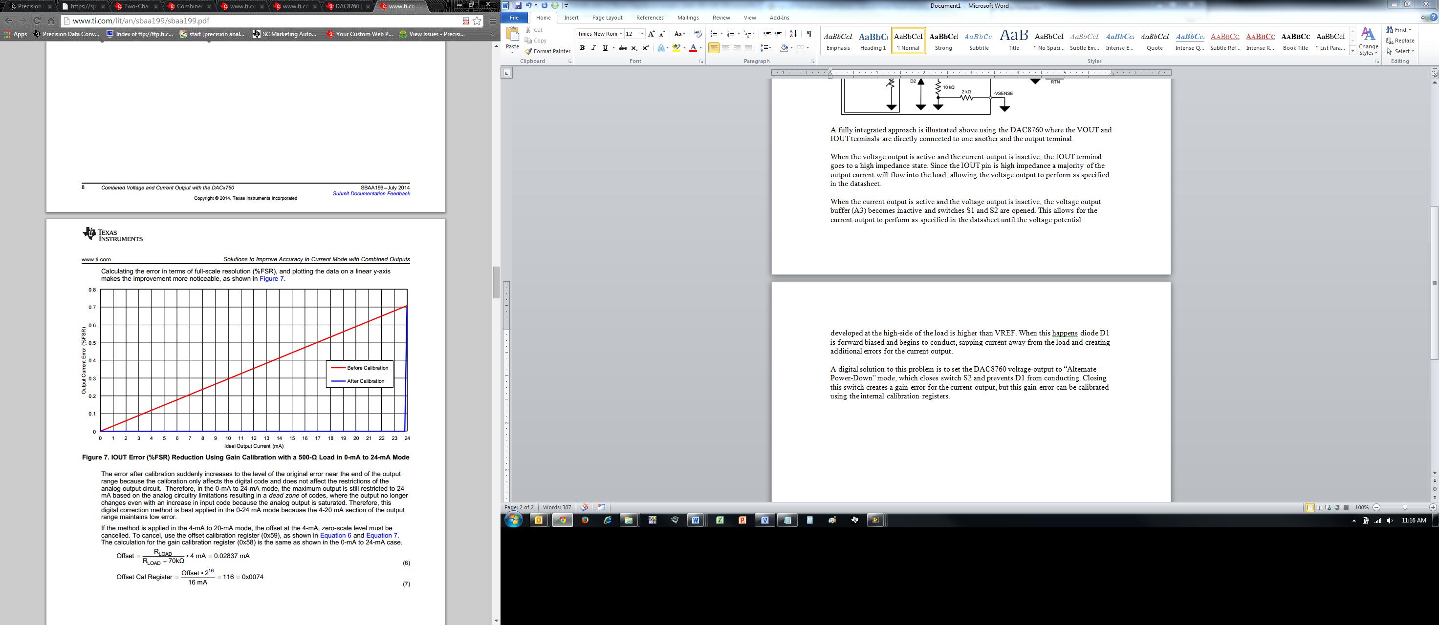
A digital solution to this problem is to set the DAC8760 voltage-output to “Alternate Power-Down” mode, which closes switch S2 and prevents D1 from conducting. Closing this switch creates a gain error for the current output, but this gain error can be eliminated using the internal calibration registers. The chart below shows the calibrated and un-calibrated results of this digital solution.
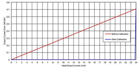
The digital solution eliminates the error introduced to the current output across the majority of the current output transfer function but this purely digital calibration techniques has limitations that results in an end-point error at full-scale.
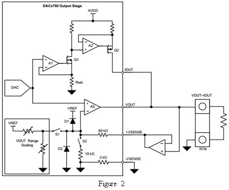
An alternate analog solution is to place a unity-gain buffer between the shared VOUT and IOUT connection and the +VSENSE connection. In this case, when the voltage at the high-side of the load reaches VREF or greater D1 will still conduct but the buffer will source this current instead of IOUT, allowing the current output to function as specified. The voltage output will be slightly impacted by the input offset voltage of the buffer, but will still maintain good performance. Check out TIPD119 for more information about this analog approach, including measured performance.
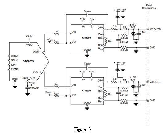
Another simple method of realizing a shared voltage and current output is a discrete approach using the XTR300 and a DAC. A two channel example of this approach is illustrated above in Figure 3. The XTR300 internal circuitry is reconfigured for voltage or current output based on digital inputs, allowing native support of a shared voltage and current output terminal. Full details of this design are discussed in TIPD155.
The next and final post in this series will turn our attention to how to build and protect 2-wire, or loop powered, analog outputs.
Related resources:
- TIPD119: Combined Voltage and Current Output Terminal for Analog Outputs (AO) in Industrial Applications
- TIPD155: Two-Channel Source/Sink Combined Voltage & Current Output, Isolated, EMC/EMI Tested Reference Design
- SBAA199: Combined Voltage and Current Output with the DACx760
- Additional posts in my Industrial DACs series
- Learn about TI’s data converter portfolio and find technical resources
