

The ΔΣ ADC is constructed from a ΔΣ modulator and a digital filter. The modulator converts the analog input into a digital bit stream, while the digital filter translates the bit stream into a data word that represents the magnitude of the analog input.
Let’s take a look at how the modulator works, starting with a very basic analysis of a first-order, ΔΣ modulator topology, as shown in Figure 1.
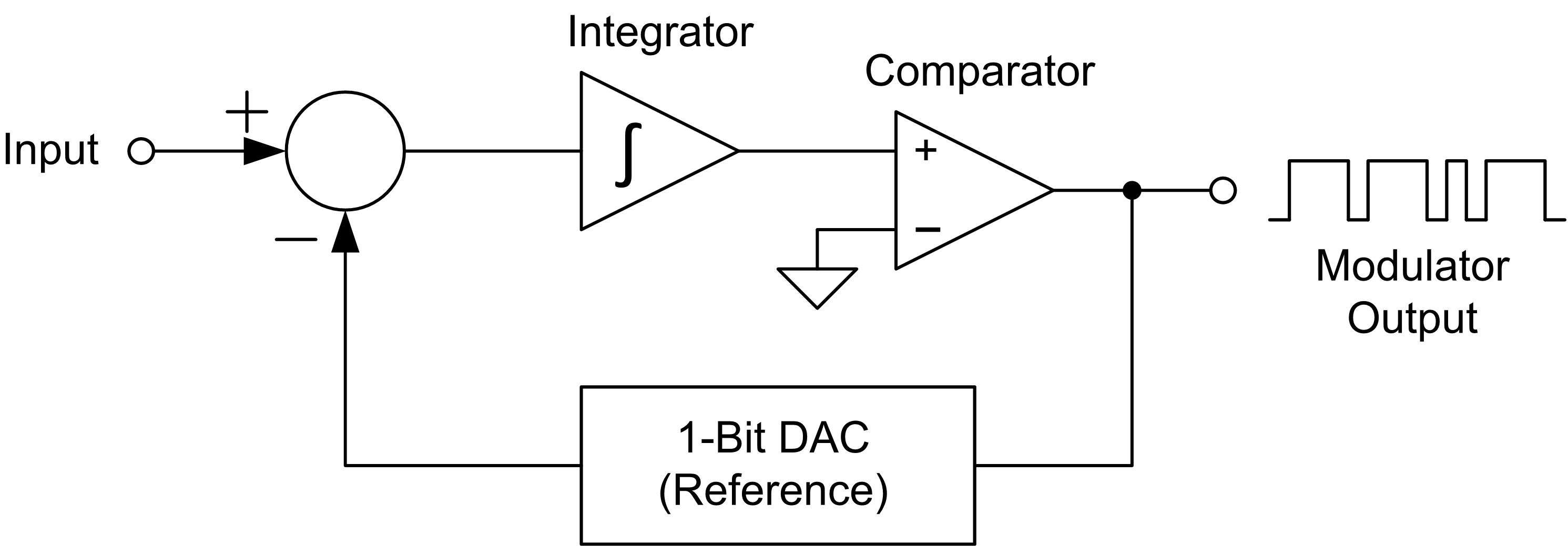
Figure 1: Delta-sigma modulator internal block diagram
The modulator runs off of the modulator clock, which determines the sampling interval of the input. The modulation loop begins by integrating the difference between the input sample and the 1-bit DAC.
The comparator determines the next modulator output based on the integrator value. Depending on the output state of the comparator, the 1-bit DAC produces a voltage equal to the positive or negative reference voltage of the ADC. If the modulator output is a 1, the reference voltage is subtracted from the input. If the output is a 0, the reference voltage is added to the input voltage. At every modulator clock pulse, the modulator completes a full cycle and generates a new output.
As the modulator clock continues to run, each modulator clock pulse will generate another modulator output pulse. The resulting output bit stream becomes a representation of the input voltage, proportional to the reference voltage. Figure 2 shows an input sine wave and the resulting modulator output bit stream, assuming a 1-V reference.
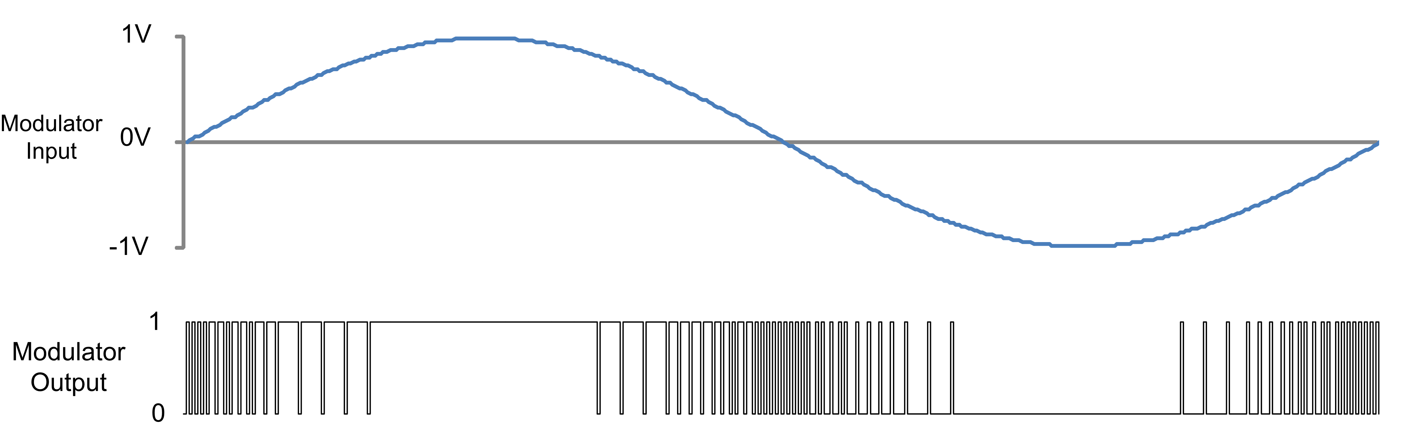
Figure 2: Sine wave input (top) and modulated output bit stream (bottom)
As the input approaches 1 V, the modulator’s bit stream approaches a 1s density of 100%. Conversely, as the input approaches -1 V, the bit stream 1s density approaches 0%. When the input is 0 V, the 1s density is 50%. Therefore, input voltages between the reference voltage and the negative of the reference voltage can be measured without over-ranging the modulator.
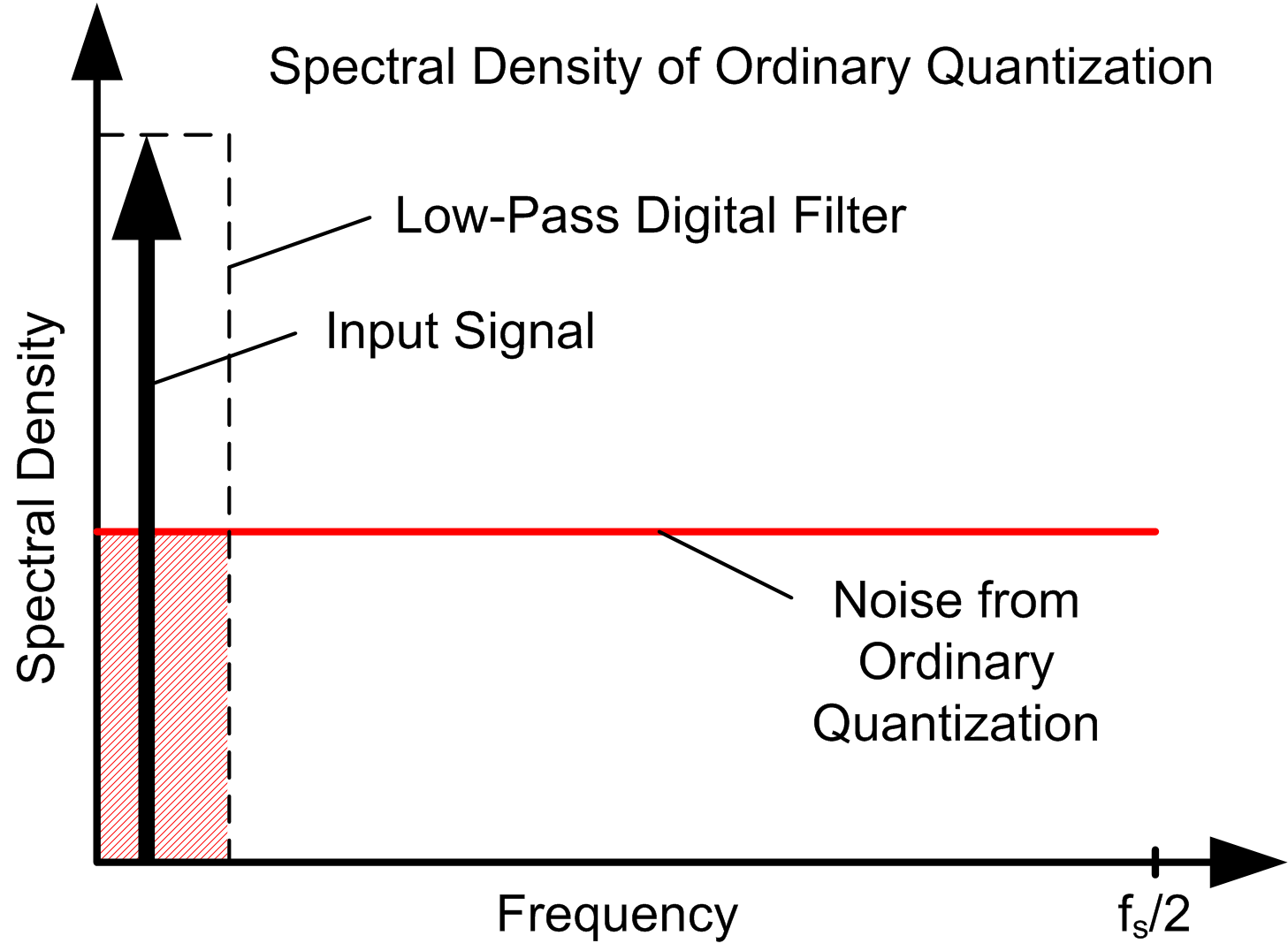
So what does the modulator achieve by converting the input into a bit stream? Looking at the spectral content of the modulator, the error between the input voltage and a sampled digital signal is modeled as a quantization noise, as shown in Figure 3a below. With simple quantization, the error spectral density is white noise from DC to the sampling frequency (fS) divided by 2.
By using ΔΣ modulation, the quantization error spectral density is shaped by pushing it to higher frequencies, shown in Figure 3b. A low-pass digital filter retains the input signal with higher resolution because the quantization noise has been moved outside the pass band of the digital filter. With ΔΣ modulation, we reduce the quantization noise and achieve a higher resolution.
 |
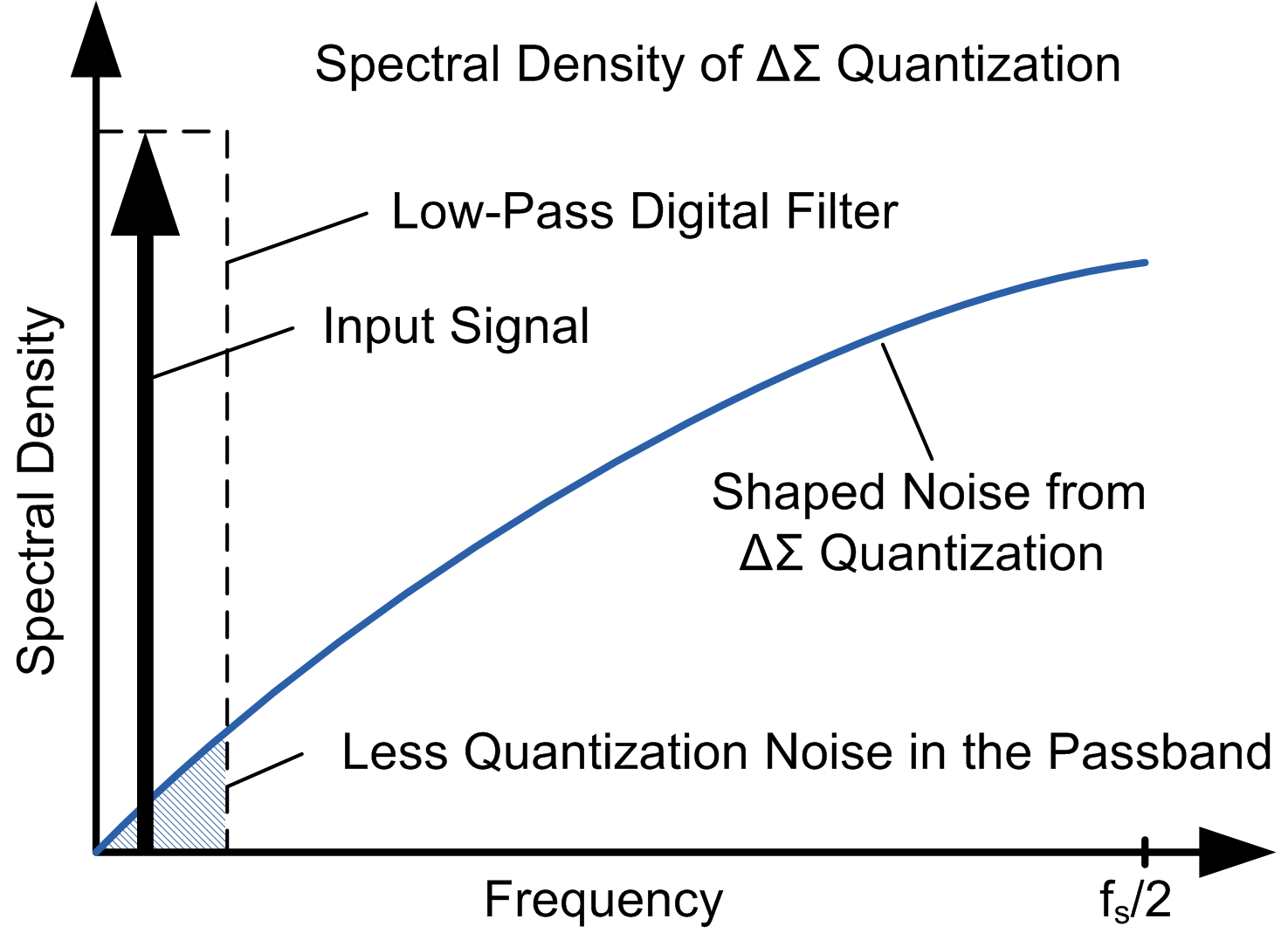 |
| Figure 3a: Noise from ordinary quantization | Figure 3b: Noise from ΔΣ quantization |
Different modulator topologies of multiple orders with additional feed-forward and feedback paths provide better noise shaping than the above basic example. Different digital filters extract the original signal and speed up the ADC with higher measurement resolution.
By breaking down this complex topology to a basic level, you can see how a ΔΣ modulator works: The modulator samples an input signal, compares it to the reference and outputs a bit stream of 1s proportional to the magnitude of the input signal compared to the reference. Be on the lookout on the Precision Hub next month, when I’ll post about how the modulator and digital filter combine to achieve greater measurement resolution.
For more in-depth information, see the following resources:
See TI’s broad range of delta-sigma ADCs.
How delta-sigma ADCs work, Part 1 by Bonnie Baker, Analog Applications Journal
How delta-sigma ADCs work, Part 2 by Bonnie Baker, Analog Applications Journal
See a video demonstration of a delta-sigma ADC in a low-power weigh scale application.